

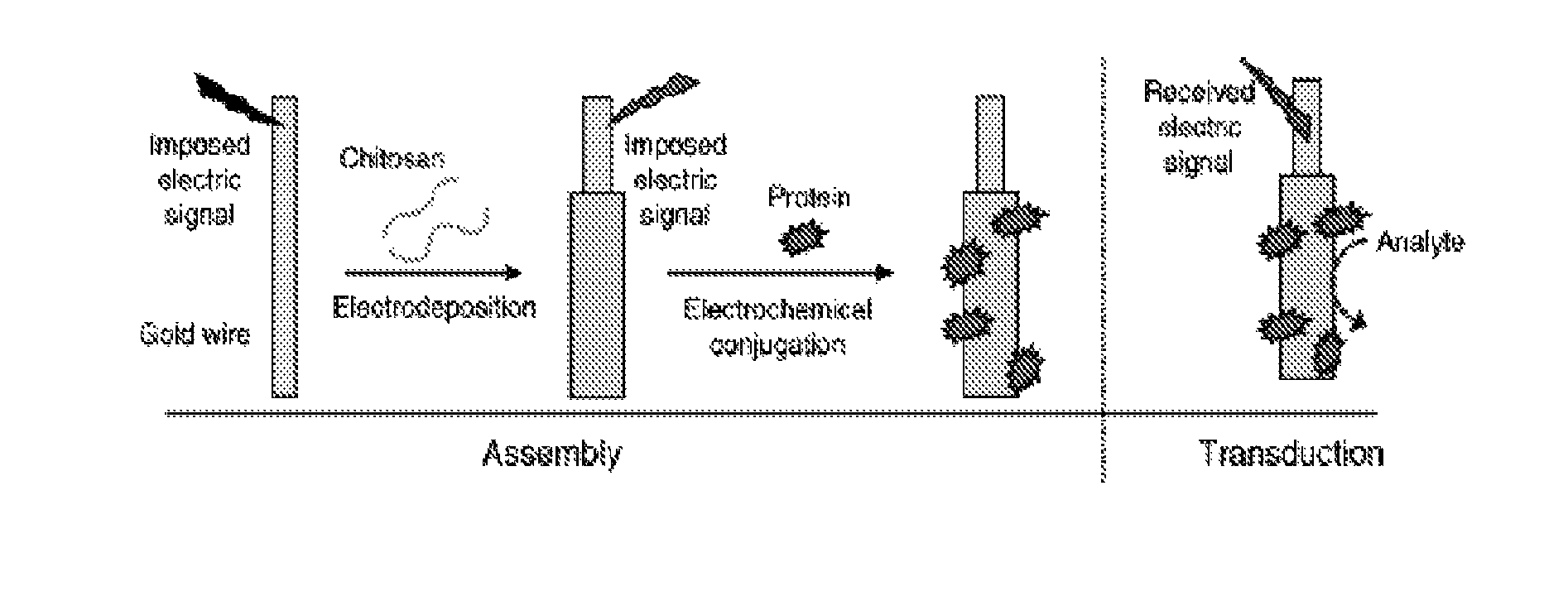
Chitosan-coated wires for biosensing
a biosensing and chitosan coating technology, applied in the field of chitosan coating wires for biosensing, can solve the problems of not always simple or benign incorporation of biological sensing elements, and the signal transduction of polymers is not as straightforward when compared to optical fibers
- Summary
- Abstract
- Description
- Claims
- Application Information
AI Technical Summary
Benefits of technology
Problems solved by technology
Method used
Image

Examples
example 1
Chitosan Electrodeposition
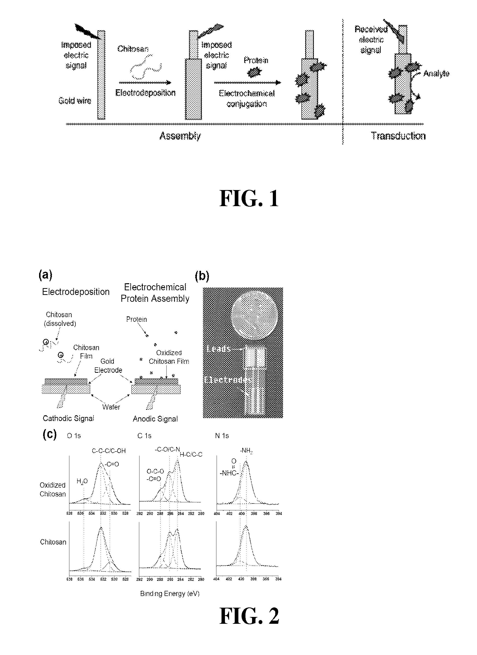
[0118]A chitosan solution (0.9 w / v %) was used for chitosan electrodeposition. This solution was prepared by adding chitosan to 1% HCl, mixing overnight, and filtering using a vacuum filter to remove undissolved particles. The pH of this chitosan solution was then adjusted to 5.6 using 1 M NaOH.
[0119]Chitosan films were electrodeposited on two adjacent electrodes of the chip in FIG. 2(b). Chemical analysis of electrochemically-activated chitosan films was performed using X-ray Photoelectron Spectroscopy (XPS). One film served as the control, while the other was anodically activated. XPS analysis was performed on a Kratos Axis 165 using Al Ka (1486.7 eV) radiation at 300 W (http: / / www.chem.umd.edu / facility / xps.php). The system was operated in the hybrid mode, survey spectra were collected with a pass energy of 160 eV and high resolution spectra at a pass energy of 20 eV. The working pressure of the instrument was at 1×10⁻⁸ Torr or better throughout data coll...
example 2
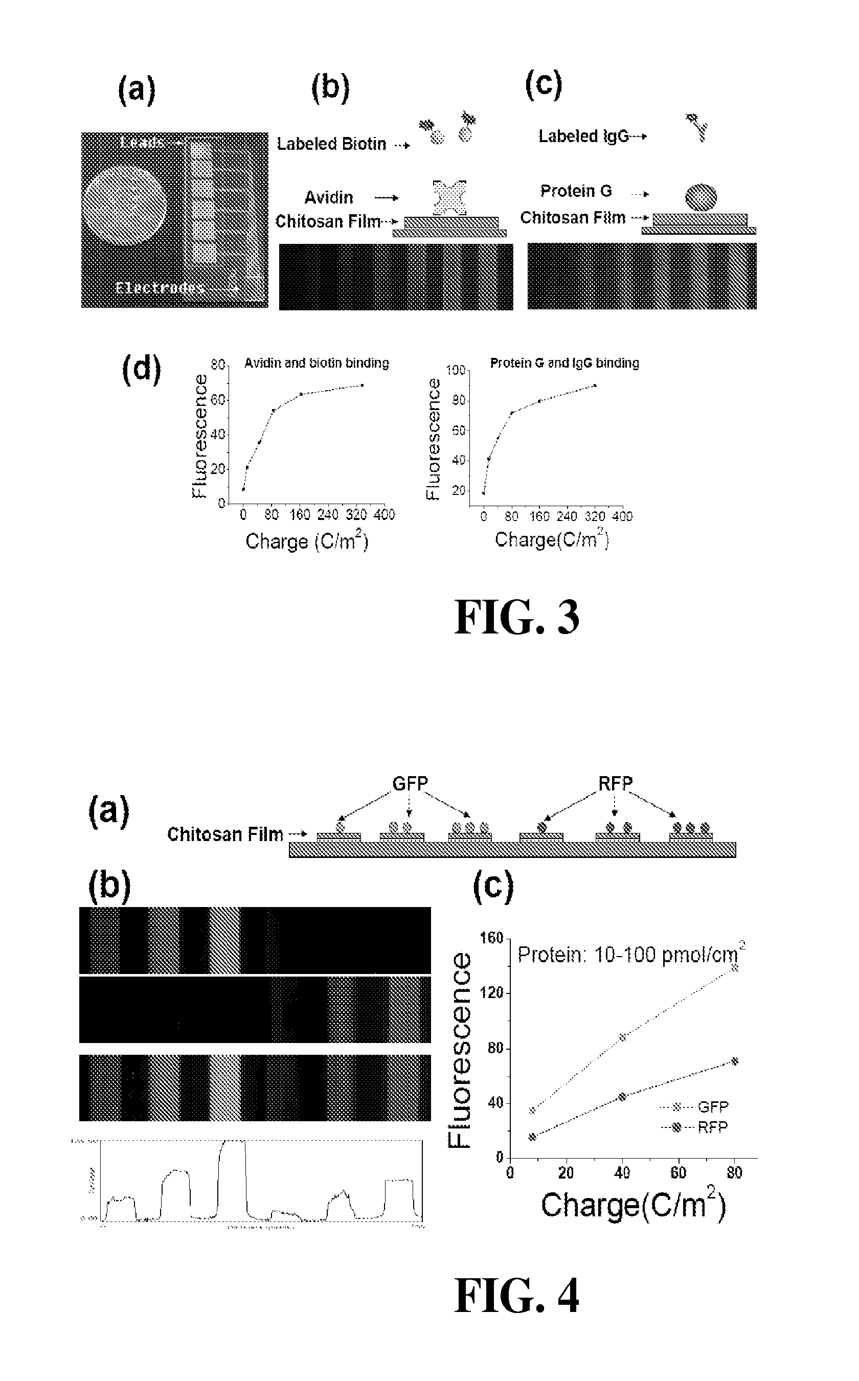
[0120]Protein assembly was performed using three steps. First, chitosan was electrodeposited by partially immersing the patterned chip into the chitosan solution (0.9%, pH 5.6), applying a cathodic voltage to achieve a constant current density of 4 A / m2 for 15 sec. After deposition, the chips were rinsed with water. The second step was to electrochemically activate the deposited chitosan film. Activation was performed by partially immersing the chips in a 0.1 M phosphate buffer (pH 7) containing 0.1 M NaCl, connecting the chitosan-coated electrode to serve as the working electrode in a 3-electrode system, and biasing the chitosan-coated electrode to an anodic voltage of 0.9 V to achieve a specific charge transfer (Q). The three-electrode system (CHI627C electrochemical analyzer, CH Instruments, Inc.) employed Ag / AgCl as the reference electrode and a Pt wire as the counter electrode. For the third step, protein conjugation to the activated films, the chips were washed...
example 3
NaCl is Required for Anodic Activation
[0121]FIG. 5 compares protein binding to chitosan films activated in 0.1 M phosphate buffer (pH=7.0) with and without NaCl. Initially, chitosan films were electrodeposited on both electrodes of the patterned chip shown in FIG. 5(a). After washing with water, the right electrode was connected to a power supply and served as the working electrode in a 3-electrode system (Ag / AgCl as a reference and Pt wire as a counter electrode) and the electrodes were immersed in 0.1 M phosphate buffer with 0.1 M NaCl. In this example, a somewhat different procedure was used to activate the chitosan film. Specifically, the potential of the underlying electrode was linearly increased from 0 to 1.5 V at rate of 100 mV-s−1. This linear increase in voltage was repeated a total of 5 times. The chitosan film on the left electrode served as a control in which the same “activation” procedure was performed in 0.1 M phosphate buffer lacking NaCl. After washing with 0.1 M P...
PUM
| Property | Measurement | Unit |
|---|---|---|
| current density | aaaaa | aaaaa |
| anodic voltage | aaaaa | aaaaa |
| pH | aaaaa | aaaaa |
Abstract
Description
Claims
Application Information