Specimen box for electron microscope
a technology of electron microscope and specimen box, which is applied in the field of specimen box for electron microscope, can solve the problems of limited application of electron microscope, limitation on specimen selection, invalidity of conventional electron microscope, etc., and achieve the effect of prolonging the in-situ observation time effectively
- Summary
- Abstract
- Description
- Claims
- Application Information
AI Technical Summary
Benefits of technology
Problems solved by technology
Method used
Image
Examples
example 1
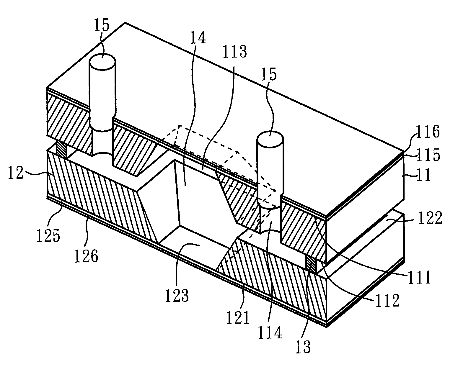
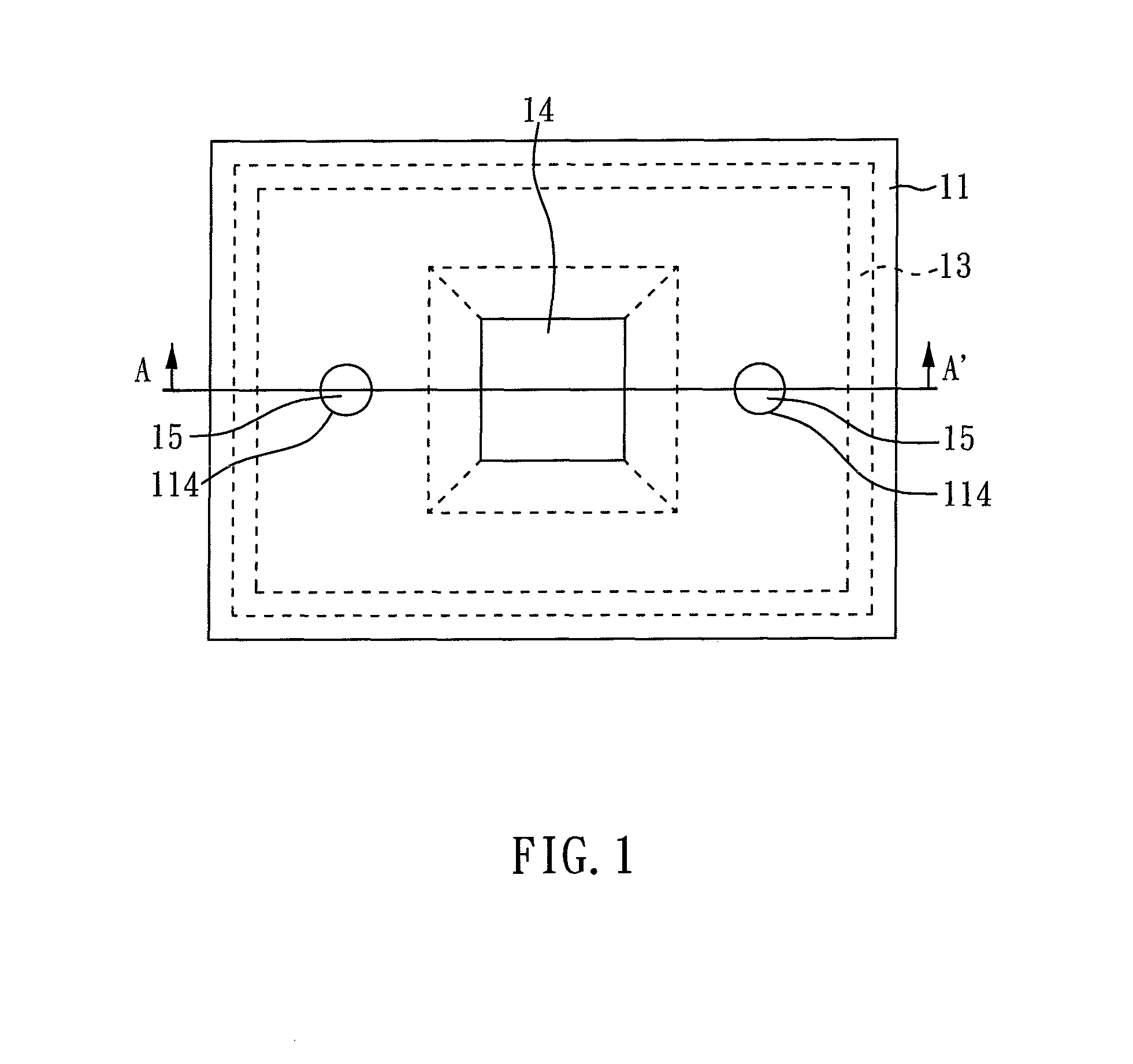
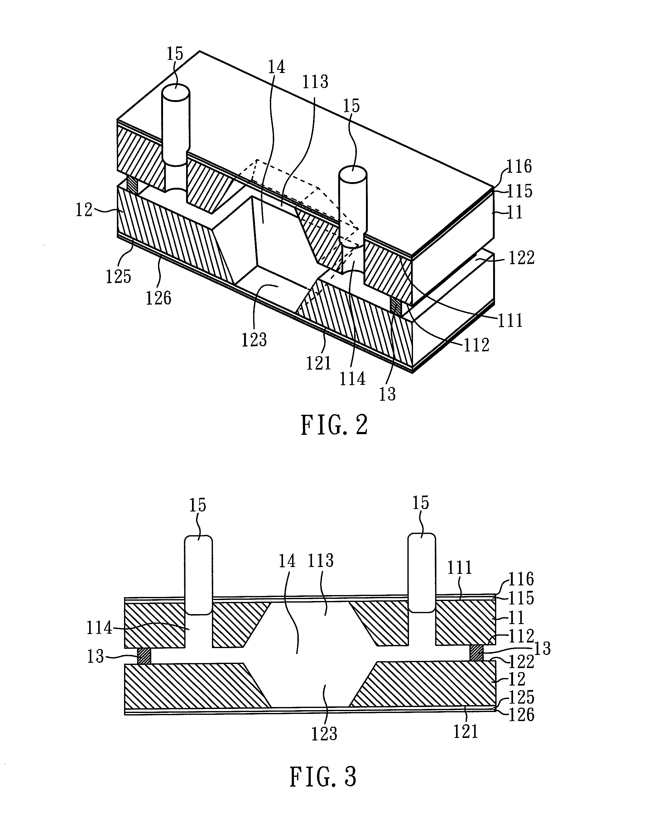
[0034]As shown in FIG. 1, FIG. 2, and FIG. 3, FIG. 1 is a top view showing the specimen box for an electron microscope of the present invention; FIG. 2 is a three-dimensional view, which along the A-A′ section line in FIG. 1, is showing the specimen box for an electron microscope of the example 1; and FIG. 3 is a perspective view, which along the A-A′ section line in FIG. 1, is showing the specimen box for an electron microscope of the example 1. According to FIG. 1, FIG. 2, and FIG. 3, the specimen box of the present invention comprises: a first substrate 11, a second substrate 12, and a metal adhesion layer 13. In the present example, the first substrate 11 and the second substrate 12 are silicon substrate. The thickness of the first substrate 11 is 250 μm, and the thickness of the second substrate 12 is also 250 μm.
[0035]The first substrate 11 has a first surface 111, a second surface 112, a first concave 113, and two first through holes 114, in which the first concave 113 is dis...
example 2
[0046]FIG. 4 is a perspective view showing the specimen box for an electron microscope of the example 2. According to FIG. 4, the specimen box of the present example is roughly the same as example 1. The only difference is the disposition of the metal adhesion layer 13. In the present example, the metal adhesion layer 13 is disposed between the second surface 112 and the second protective layer 126, in which the material of the metal adhesion layer 13 is Sn—In eutectic solder.
[0047]The volume of the space 14 in the present example is 2 mm3. In the present example, the volume of the space 14 is smaller than example 1, so the resolution is higher than example 1. Therefore, different volumes of the space 14 of the specimen box could be chosen according to different requirements of the observation, such as the volume of the specimen, and the required resolution.
example 3
[0048]FIG. 5 is a perspective view showing the specimen box for an electron microscope of the example 3. According to FIG. 5, the specimen box of the present example is roughly the same as example 1 and example 2. The only difference is the disposition of the metal adhesion layer 13. The metal adhesion layer 13 is disposed between the first protective layer 116 and the second protective layer 126 to form a space14 with the volume of 0.02 mm3. The volume of the space 14 is smaller than the space 14 of example 1 and example 2 so the resolution is higher than example 1 and example 2. Therefore, different volumes of the space 14 of the specimen box could be chosen according to different requirements of the observation, such as the volume of the specimen, and the required resolution.
[0049]Furthermore, in the present example, the second through holes 124 are formed by deep reactive-ion etching process, and the second through holes 124 are penetrated through the second thin film 125 and th...
PUM
 Abstract
Description
Claims
Application Information


