Write assist in a dual write line semiconductor memory

a write assist and semiconductor memory technology, applied in the field of data storage, can solve the problems of increasing the size of devices and power consumption, instability in bit cells and bit cell flipping values, and the inability to design robust semiconductor memories such as sram, so as to overcome the stability of the feedback loop, less charge injection, and less chance of the stored value being corrupted

Active Publication Date: 2013-11-12
ARM LTD
View PDF6 Cites 15 Cited by
  • Summary
  • Abstract
  • Description
  • Claims
  • Application Information

AI Technical Summary

Benefits of technology

[0011]The present invention recognises the difficulties of being able to write successfully to a cell when it may be operating at ever lower voltages, higher speeds and smaller topologies. It addresses this problem by configuring a cell to have two data lines and two access control lines, in a similar way to a dual port storage device, but rather than using the two independently it uses them together to write one value to a cell. This arrangement is analogous to increasing the width of the first access control device of the cell being written to and allows the charge to be transferred more effectively to the cell, thereby increasing the probability of the write being successful. Furthermore, there is no need to provide an increased voltage to an access control line, rather the two access control lines simply have the same signal applied to them to allow access to two data lines holding the same data value.
[0043]A bit cell which has access control devices that provide access to one data line that are larger than the access control devices providing access to another data line can be advantageous where the secondary data line is simply used as a write assist data line and the primary data line is used both for read and write. Thus, it may be advantageous to design such cells with one access control device that is larger than the other as this access control device has more effect on performance than the other access control device.

Problems solved by technology

With ever increasing demands to reduce both the size of devices and their power consumption, it is becoming increasingly challenging to design robust semiconductor memories such as SRAM.
However, the difference in voltage levels between the precharged bit line and the 0 may result in the node storing a 0 being pulled up towards 1 resulting in instability in the bit cell and the bit cell flipping value.
As dimensions scale down the variations in device properties due to random dopant fluctuations, line edge roughness etc. increase drastically thereby causing an increase in the rate of read disturbs as well as reduced write margins, with smaller scale geometries.
Thus, designing a robust SRAM where cells can be read (without read disturb) and written to across all operational voltage ranges turns out to be difficult.
Reducing the voltage at which the SRAM cells can be read and written to successfully is not easy and in particular as the voltage scales down it becomes increasingly difficult to write to the cells.
Write assist mechanisms that increase the voltage on the word line during a write to improve access are known but such techniques have the disadvantage of increasing the probability of a read disturb to a cell on the same row as the cell being accessed and require the provision of an additional higher voltage level.

Method used


Image

  • Write assist in a dual write line semiconductor memory
  • Write assist in a dual write line semiconductor memory
  • Write assist in a dual write line semiconductor memory

Examples


Embodiment Construction

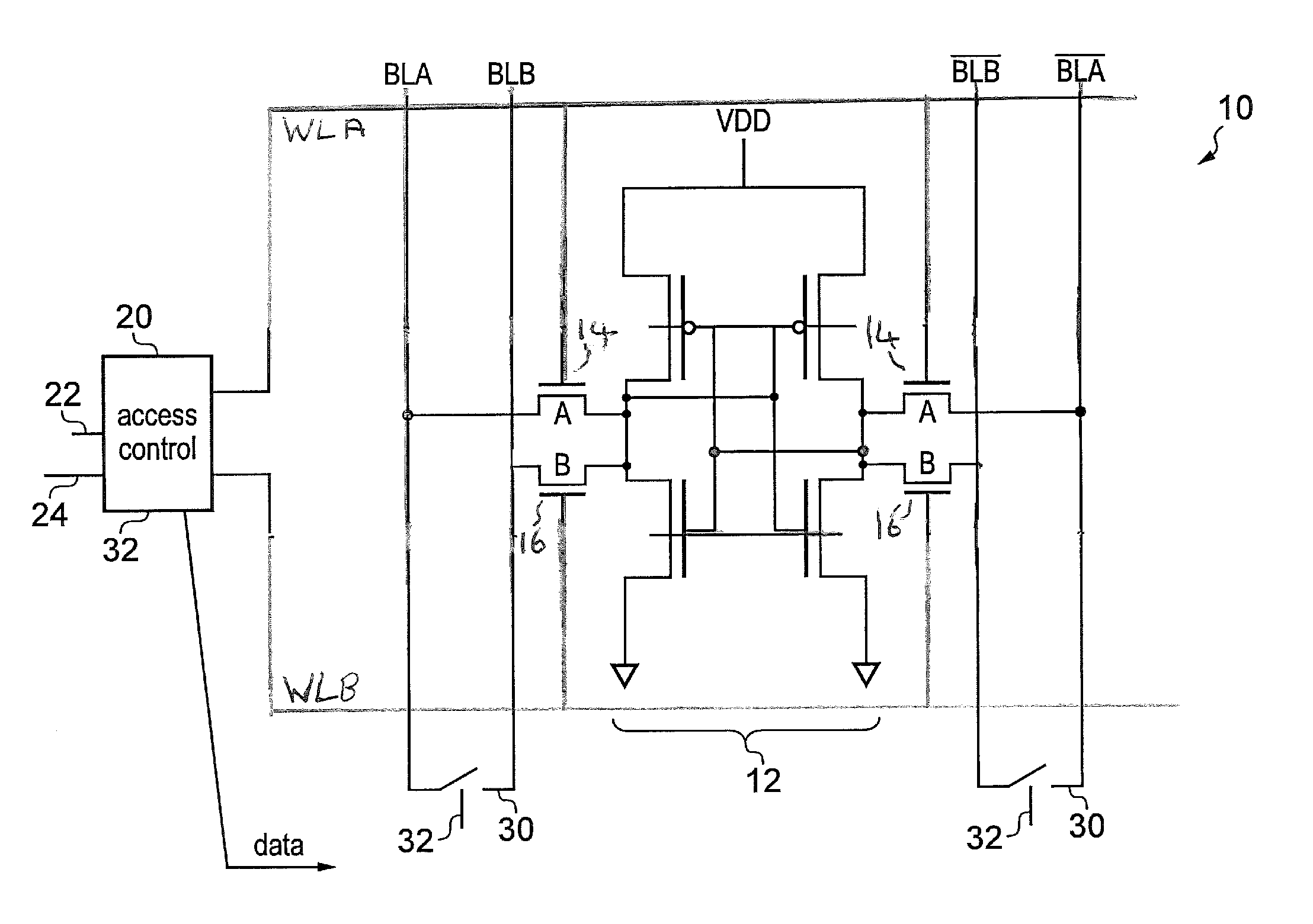
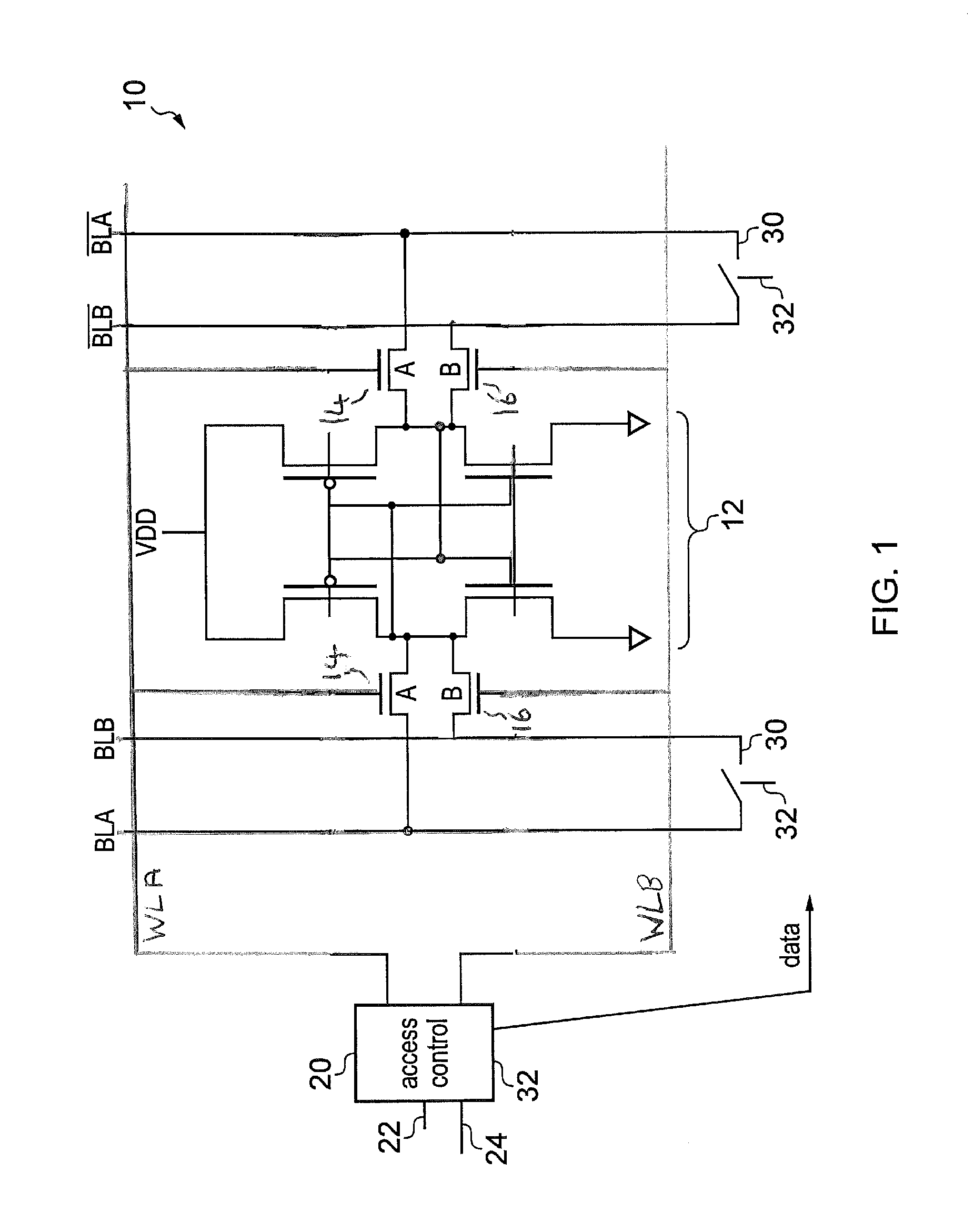
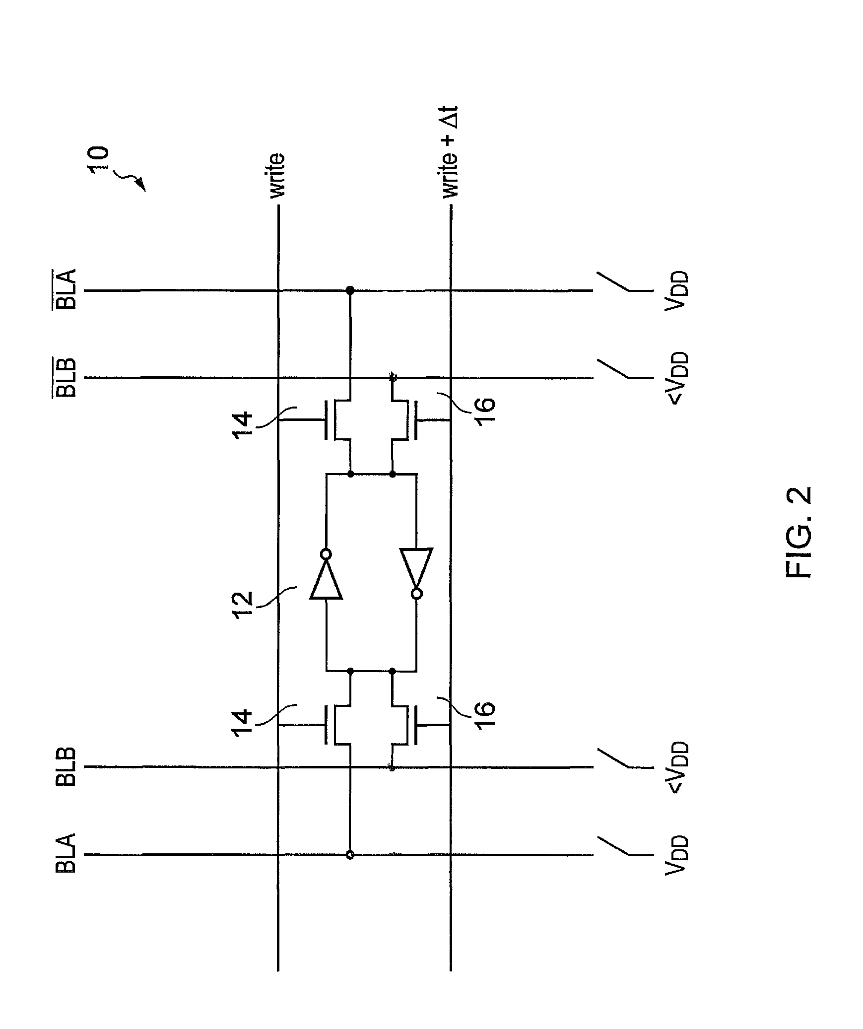
[0055]FIG. 1 shows a storage cell 10 in a memory comprising a feedback loop 12 for storing a data value and two sets of access transistors 14 and 16.

[0056]Access transistors 14 provide access to bit line and complimentary bit line A and are controlled by word line A while access transistors 16 provide access to bit line and complimentary bit line B and are controlled by word line B. The memory also comprises access control circuitry 20 which generates the access control signals and applies them to the word lines in response to an access request received at input 22.

[0057]Storage cell 10 is configured in a similar way to a conventional dual port storage cell but is configured with access control circuitry 20 and switching circuitry 30 that allows it to operate in a single port mode with the secondary data lines BLB and word line WLB being used to increase the writeability of the cell rather than to provide an additional data port. It may be configured to operate in this mode for all ...


PUM


Abstract

A semiconductor memory storage device with a plurality of storage cells, each cell includes two access control devices, each providing the cell with access to or isolation from a respective one of two data lines in response to an access control signal provided by access control circuitry. The control devices are controlled to provide the storage cell with access to or isolation from either of the first and second of the two data lines. The access control circuitry is responsive to a data access request, the data access request being a write request, to apply a data value to be written to both of the first and second data lines and to apply the access control signal to both of the first and second access control lines.

Description

BACKGROUND OF THE INVENTION[0001]1. Field of the Invention[0002]The field of the invention relates to the field of data storage and in particular, to the storage and access of data in semiconductor memories.[0003]2. Description of the Prior Art[0004]With ever increasing demands to reduce both the size of devices and their power consumption, it is becoming increasingly challenging to design robust semiconductor memories such as SRAM. Each storage cell in an SRAM comprises a feedback loop for holding a data value. In order to write to the feedback loop and store a new value, the input data value must have a high enough voltage level to be able to switch the state stored by the feedback loop if required, while reading from the feedback loop should be performed without disturbing the values stored in any of the feedback loops.[0005]SRAM bit cells are generally designed to be small and can conventionally be built from 6 transistors. However, dual port cells are also known that are built ...

Claims


Application Information

Patent Timeline
Patent Type & Authority Patents(United States)
IPC IPC(8): G11C7/12
CPCG11C7/12G11C8/16G11C11/419G11C7/10G11C7/22
Inventor GAJJEWAR, HEMANGI UMAKANTIDGUNJI, SACHIN SATISHYEUNG, GUS
Owner ARM LTD
Why Eureka
Try Eureka