Semiconductor device performing signal transmission by using inductor coupling

a technology of inductance coupling and semiconductor devices, applied in transmission systems, using reradiation, instruments, etc., can solve the problems of limited limit the efforts to microfabricate transistor devices, and limit the number of wires that can be used, so as to reduce the transmission power of semiconductor devices and achieve high-quality signal transmission. , the effect of increasing the transmission distan

Inactive Publication Date: 2013-11-19
NEC CORP
View PDF28 Cites 3 Cited by
  • Summary
  • Abstract
  • Description
  • Claims
  • Application Information

AI Technical Summary

Benefits of technology

[0027]It is an object of the present invention to provide a semiconductor device which reduces the effect of characteristic variations caused when semiconductor devices are manufactured, does not require highly accurate positioning control, and is capable of performing high-quality signal transmission.
[0028]Another object of the present invention is to provide a semiconductor device which efficiently receives a signal generated by a transmission coil for reducing the consumption of power.Means for Solving the Problems
[0032]According to the present invention, the processing process of an arithmetic device of signal receivers, or the signals of a transmission signal generator of signal transmitters, or both are controlled after they are mounted on chips, to remove the effect of positional displacements caused when they are mounted on the chips, the effect of offsets due to variations caused when the semiconductor device is manufactured, and the effect of disturbances, to thereby perform high-quality signal transmission.
[0033]Since the signals transmitted by the transmitters can effectively be utilized, the transmission power of the semiconductor device can be reduced, and the transmission distance can also be increased.

Problems solved by technology

The first reason for this is that semiconductor chips are more required to have multifunctionality and large storage capacity than transistor devices that are microfabricated to increase multifunctionality and storage capacity, and the second reason is that there are limitations on efforts to microfabricate transistor devices.
However, the wire bonding approach poses some problems.
First, the number of wires that can be used is limited because each pad requires a certain pad area of 100 μm squared, for example.
Secondly, pads on the surfaces of semiconductor chips need to be mounted on the outer sides of the layered chips so that the pads can be connected from outside of the chips.
If identically shaped semiconductor chips are layered, then the bonding wire pads may not be made available.
Therefore, the semiconductor fabrication process is complex or is highly costly and time-consuming.
As a result, the chips that can be layered are limited to two layers, and there are limitations on the layering of three or more chips and on efforts to achieve multifunctionality and larger storage capacity.
According to the above relevant art, it is very difficult to mount the chips while they are kept in highly accurate relative positions.
Even if the chips can be mounted highly accurately, the packaging cost is increased.
Furthermore, since the coil positions cannot be changed once the chips have been mounted in position, the transmission rate is limited, and the error rate cannot be sufficiently lowered.
Therefore, the manufacturing cost of the signal transmitting apparatus has been high.
Furthermore, device characteristic variations caused when semiconductor devices are manufactured make it impossible to sufficiently lower the error rate in signal transmission.
For example, if there are characteristic variations between the transistors of the receiver, then they make the receiver behave as if an offset has been added to the input signal, tending to lead to an erroneous transmission of the signal.
Accordingly, any magnetic fluxes that spread away from the magnetic fluxes that are directed directly below the transmission coil and pass through the reception coil are wasted.

Method used


Image

  • Semiconductor device performing signal transmission by using inductor coupling
  • Semiconductor device performing signal transmission by using inductor coupling
  • Semiconductor device performing signal transmission by using inductor coupling

Examples


1st exemplary embodiment

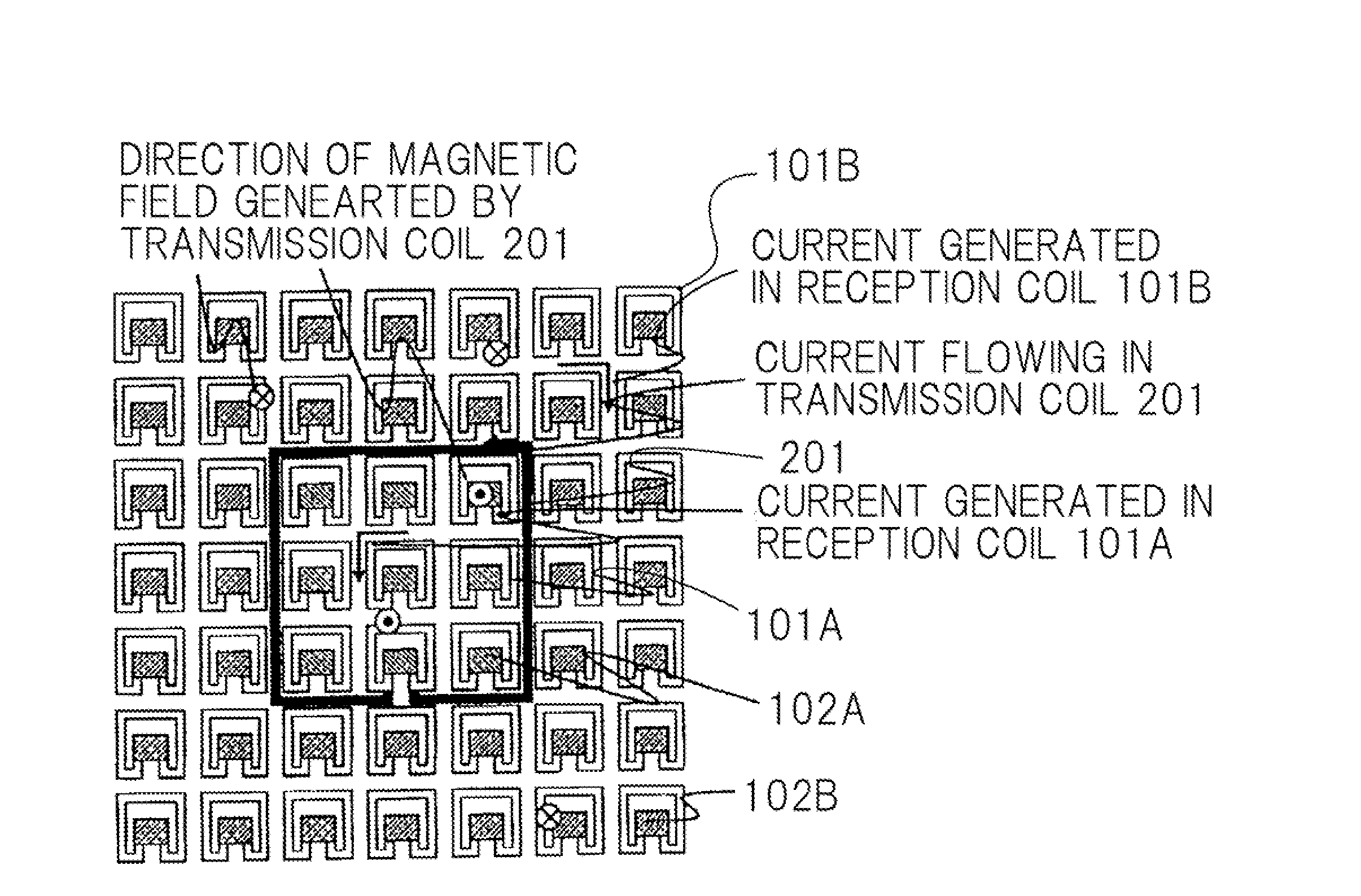
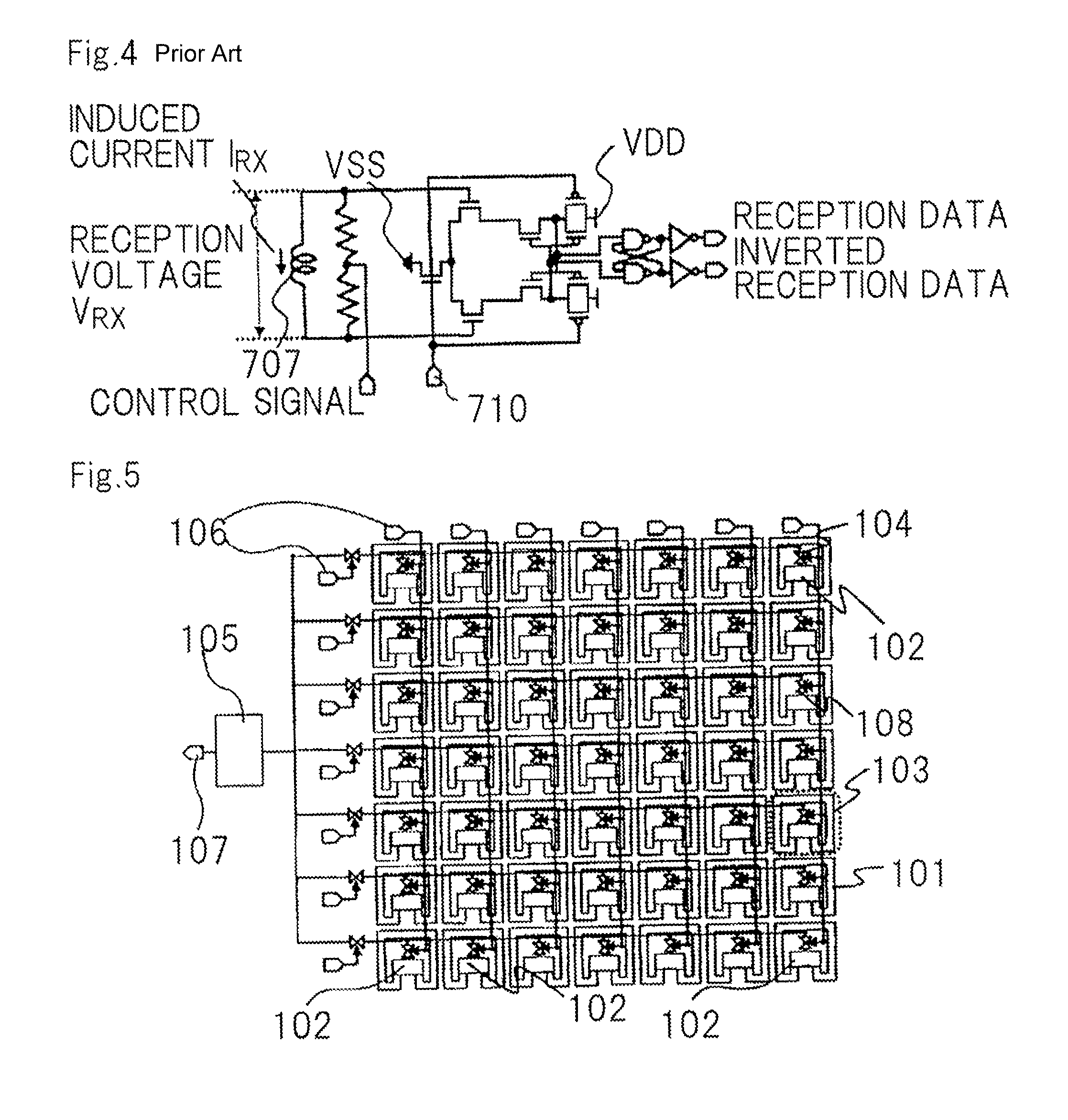
[0105]FIG. 5 is a block diagram of a receiving section of a semiconductor device according to a first exemplary embodiment of the present invention, i.e., a semiconductor device having a transmission and reception coil pair comprising a single transmission coil and a plurality of reception coils.

[0106]The receiving section includes a plurality of reception mechanisms 103 in an array of seven rows×seven columns, each of reception mechanisms 103 comprising reception coil 101 and signal receiver 102. Signals received by reception mechanisms 103 are sent from readers 104 that are controlled by read control signals 106 to arithmetic device 105, which process the received signals into reception data 107. It is assumed that signal receiver 102 at the mth×nth location in FIG. 5 is referred to as R(m,n) and output signal 108 from R(m,n) is referred to as D(m,n) where m represents an mth row and n represents an nth column, each of m, n being an integer of 0 or greater than 0. In FIG. 1, each ...


PUM


Abstract

Disclosed is a semiconductor device which performs signal transmission by using inductor coupling. The semiconductor device comprises one or more transmission and reception coil pair, each pair comprising a single transmission coil and a plurality of reception coils, or a plurality of transmission coils and a single reception coil, or a plurality of transmission coils and a plurality of reception coils.

Description

[0001]The present application is the National Phase of PCT / JP2008 / 052877, filed Feb. 20, 2008, which claims priority based on Japanese patent application No. 2007-043561 filed on Feb. 23, 2007, and incorporates herein the disclosure thereof by way of reference.TECHNICAL FIELD[0002]The present invention relates to a semiconductor device, and more particularly to a semiconductor device for transmitting a signal through an electromagnetic coupling provided by an electromagnetic inductance coil (inductive coupling) between chip layers which are stacked in a vertical direction.BACKGROUND ART[0003]Semiconductor integrated circuits have had their integration density increased by efforts to microfabricate transistor devices which make up the semiconductor integrated circuits. Semiconductor integrated devices on single chips have begun incorporating multifunctionality. Semiconductor memory devices have also had their storage capacity increased regardless of their types, such as DRAM (Dynamic...

Claims


Application Information

Patent Timeline
Patent Type & Authority Patents(United States)
IPC IPC(8): H04B5/00H04B1/06G08C19/12H04B7/00H04B1/16G01V3/00G08C19/06
CPCH01L23/48H01L25/0657H04B5/0087H01L2225/06527H01L2924/0002H01L2924/00
Inventor NAKAGAWA, YOSHIHIRO
Owner NEC CORP
Why Eureka
Try Eureka