

Boosting circuit and RFID tag including boosting circuit
a boosting circuit and boosting circuit technology, applied in the direction of electric variable regulation, process and machine control, instruments, etc., can solve the problems of insufficient boosting due to capacitive coupling and the reduction of the potential boosted in each unit boosting circuit, so as to reduce the potential, enhance the boosting efficiency, and prevent the effect of the output potential of the unit boosting circui
- Summary
- Abstract
- Description
- Claims
- Application Information
AI Technical Summary
Benefits of technology
Problems solved by technology
Method used
Image

Examples
embodiment 1
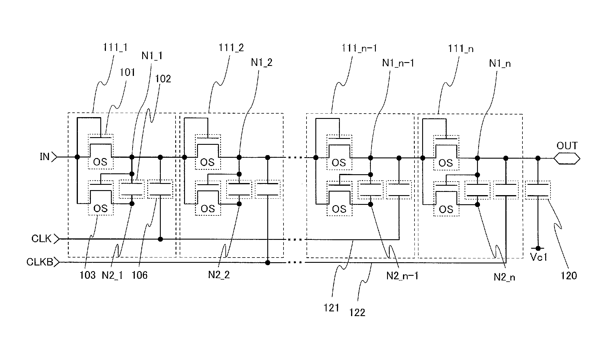
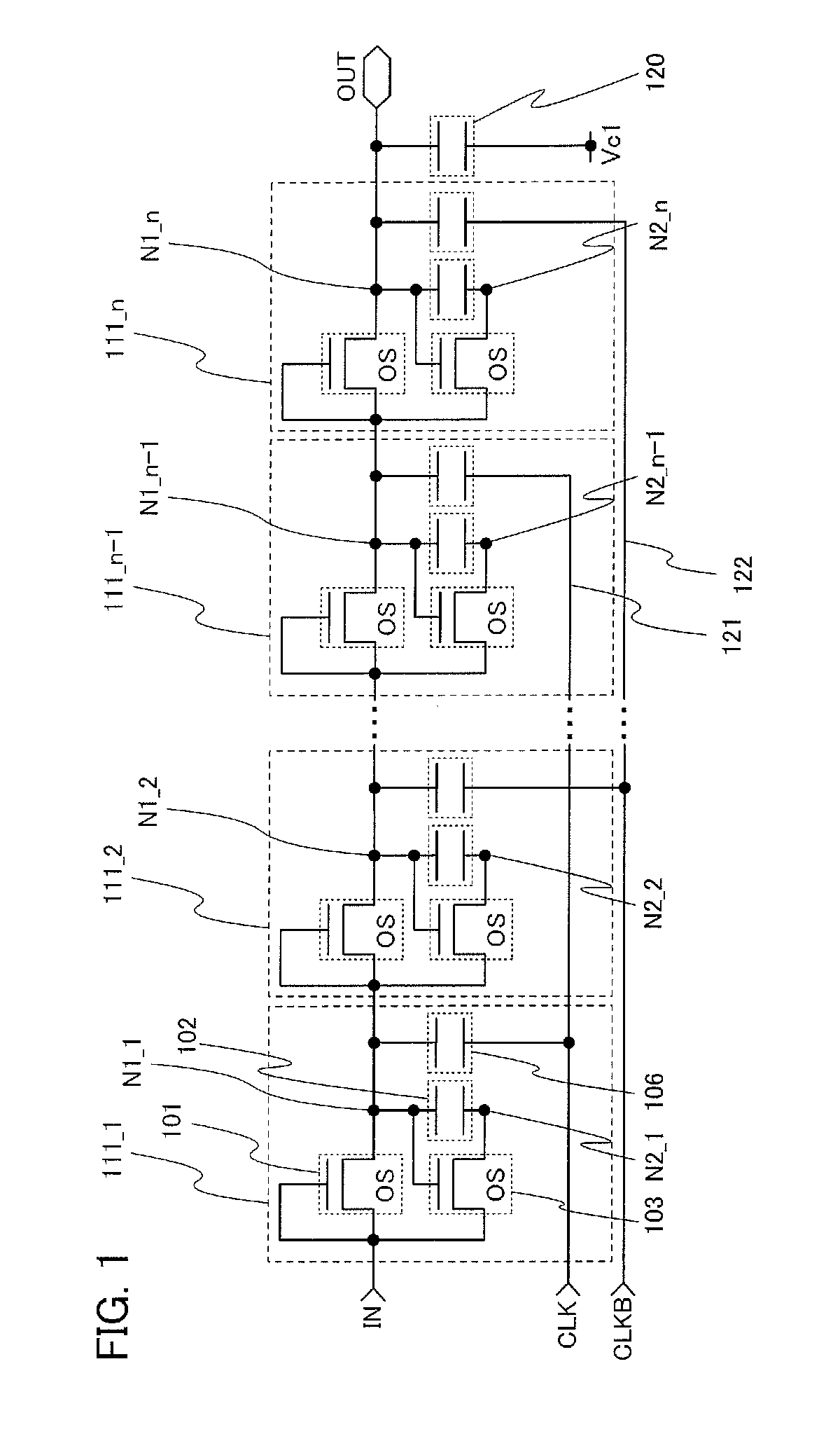
[0047]In this embodiment, a boosting circuit according to one embodiment of the disclosed invention will be described with reference to FIG. 1, FIG. 2, and FIG. 3. Note that in a circuit diagram, “OS” may be written beside a transistor in order to indicate that the transistor includes an oxide semiconductor.
[0048]An example of a circuit configuration of a boosting circuit according to one embodiment of the disclosed invention will be described with reference to a circuit diagram of FIG. 1.
[0049]A boosting circuit illustrated in FIG. 1 is formed with n stages of unit boosting circuits 111_1 to 111—n (n is a natural number) which are electrically connected to each other in series. Here, a unit boosting circuit forms one stage of the boosting circuit.
[0050]Each of the unit boosting circuits 111_1 to 111—n includes a transistor 101, a capacitor 102, a transistor 103, and a capacitor 106. Note that in the case where the electrostatic capacitance of a gate insulating layer of the transist...
embodiment 2
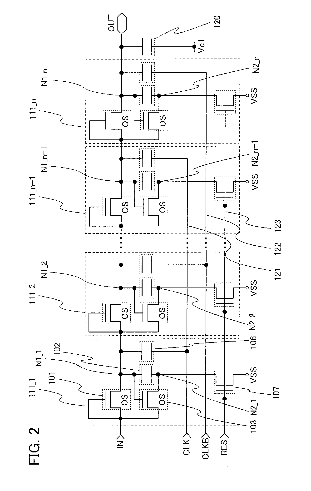
[0095]In this embodiment, a boosting circuit which differs from the boosting circuit described in Embodiment 1 will be described with reference to FIG. 4 and FIG. 5. Note that in a circuit diagram, “OS” may be written beside a transistor in order to indicate that the transistor includes an oxide semiconductor.
[0096]An example of a circuit configuration of a boosting circuit according to one embodiment of the disclosed invention will be described with reference to a circuit diagram of FIG. 4.
[0097]A boosting circuit illustrated in FIG. 4 is formed with n stages of unit boosting circuits 211_1 to 211—n (n is a natural number) which are electrically connected to each other in series. Here, a unit boosting circuit forms one stage of the boosting circuit.
[0098]Each of unit boosting circuits 211_1 to 211—n includes a transistor 201, a capacitor 202, a transistor 203, a transistor 204, a transistor 205, a capacitor 206, and an analog switch 215 including first to fourth terminals. Note tha...
embodiment 3
[0150]In this embodiment, an RFID tag that is an application example of the boosting circuits in the above embodiments will be described with reference to FIG. 6.
[0151]An RFID tag in this embodiment includes a memory circuit inside, stores information which is necessary for the memory circuit, and transmits and receives information to / from the outside by using contactless means, for example, wireless communication. With these characteristics, an RFID tag can be used for an individual authentication system in which an object or the like is recognized by reading the individual information, for example. In order that an RFID tag is used for such application, extremely high reliability is needed.
[0152]A structure of an RFID tag will be described with reference to FIG. 6. FIG. 6 is a block diagram illustrating the structure of the RFID tag.
[0153]As illustrated in FIG. 6, an RFID tag 300 includes an antenna 304 which receives a radio signal 303 transmitted from an antenna 302 connected to...
PUM
 Abstract
Description
Claims
Application Information