Soldering material and electronic component assembly

a technology of electronic components and soldering materials, which is applied in the direction of soldering apparatus, sustainable manufacturing/processing, final product manufacturing, etc., can solve the problems that the conventional lead-free solder described above does not have a satisfactory thermal fatigue resistance for an application, and achieve the effect of improving the thermal fatigue resistan

Active Publication Date: 2013-12-03
PANASONIC CORP
View PDF26 Cites 9 Cited by
  • Summary
  • Abstract
  • Description
  • Claims
  • Application Information

AI Technical Summary

Benefits of technology

[0030]Further, according to the present invention, an electronic component assembly which already has a blocking structure by an intermetallic compound, which contributes to improvement in a thermal fatigue resistance, can be produced intentionally.

Problems solved by technology

However, conventional lead-free solders as described above do not have a satisfactory thermal fatigue resistance for an application subjected to such severe temperature environment.

Method used


Image

  • Soldering material and electronic component assembly
  • Soldering material and electronic component assembly
  • Soldering material and electronic component assembly

Examples


examples

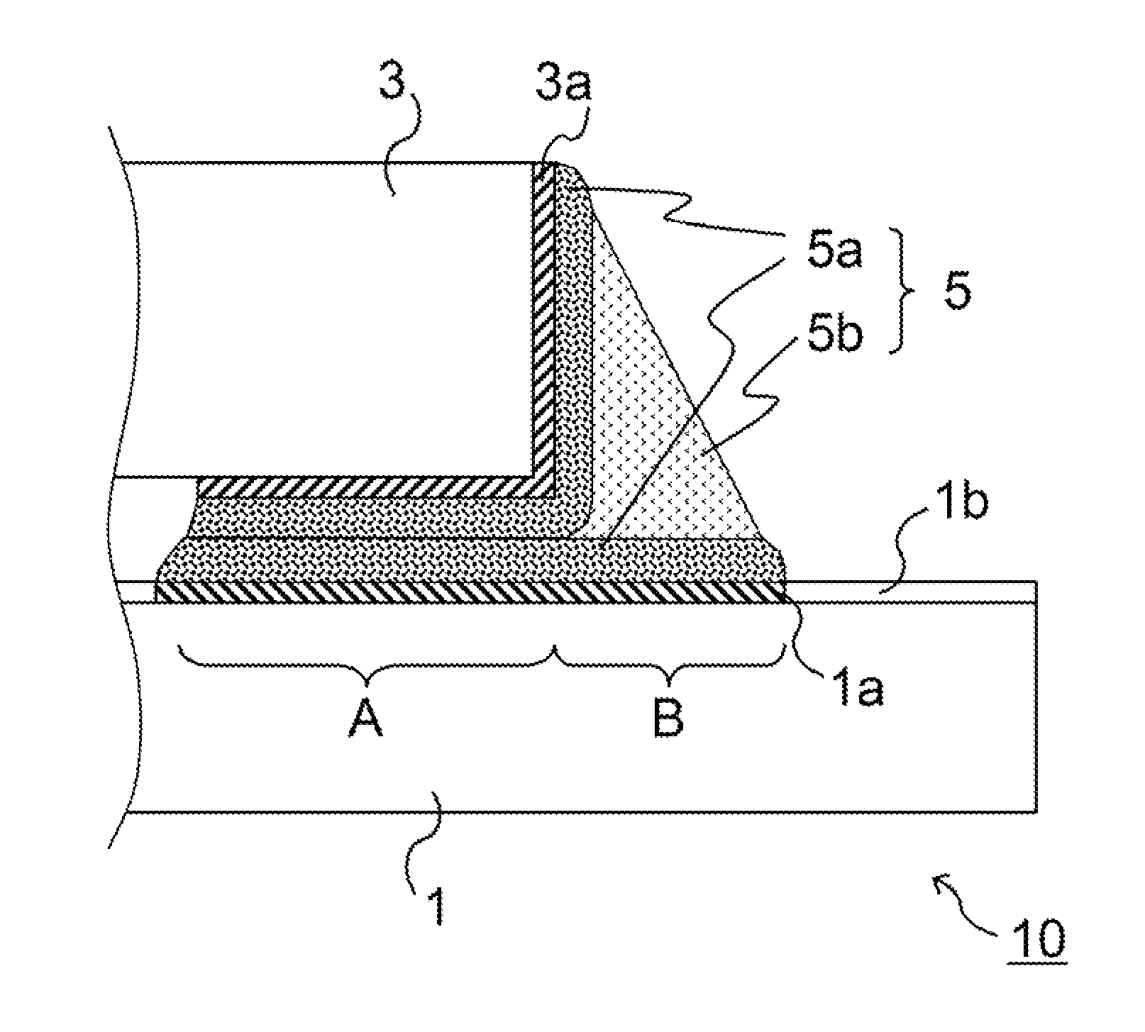
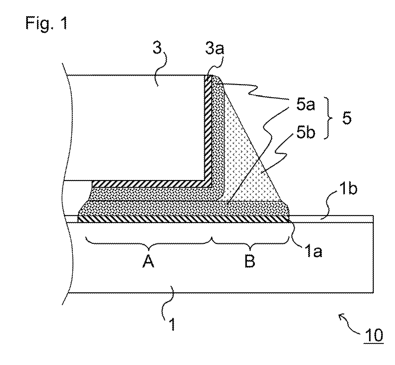
[0109]With the use of a solder material having various metal compositions shown in Tables 2 and 3, an electronic component assembly shown in FIG. 1 was prepared according to the flow diagram of steps explained above with reference to FIG. 6(a) under conditions below. In Tables 2 and 3, “Bal.” means remainder (balance).

[0110]Substrate 1: High Tg type, high heat resistant substrate R-1755T, double-sided with copper, thickness of 1.2 mm (Panasonic Electric Works Co., Ltd.)

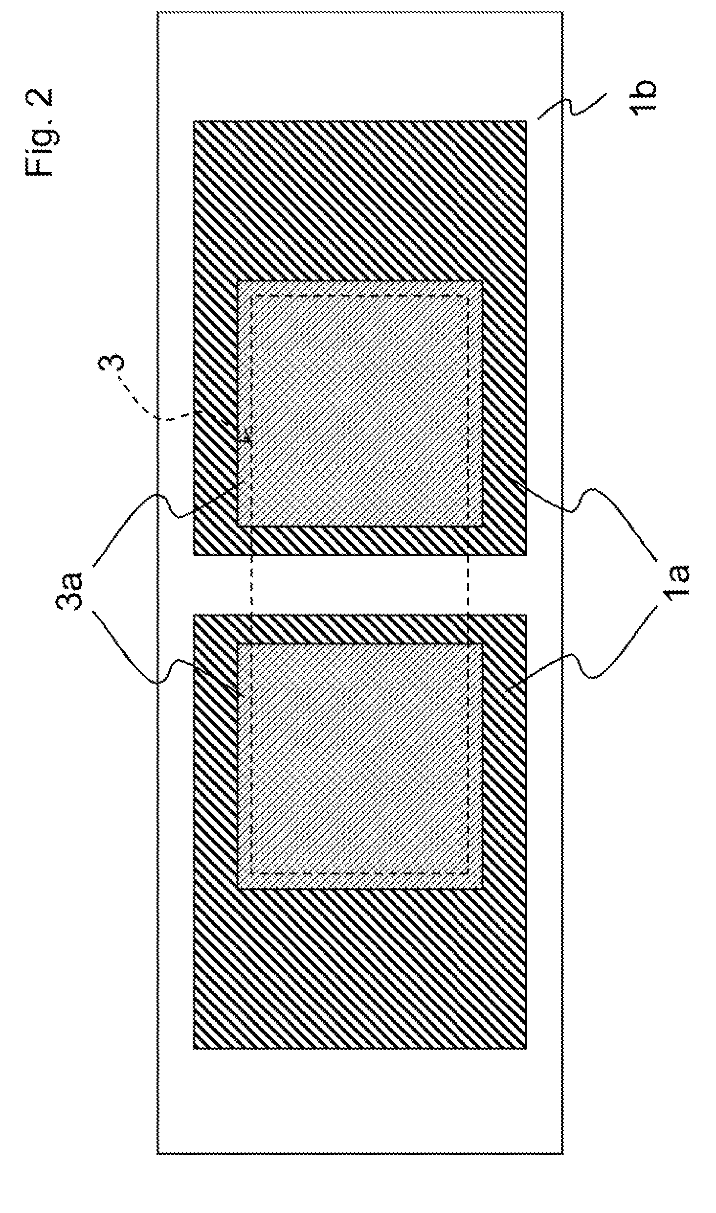
[0111]Electronic land 1a: Cu land, thickness of 35 μm, having subjected to surface treatment by a pre-flux preparation agent (“Tough-Ace”, SHIKOKU CHEMICALS CORPORATION)

[0112]Resist 1b: High heat resistant resist (TAIYO INK MFG. CO., LTD.)

[0113]Electronic component 3: Chip capacitor, size of 1005, (TDK Corporation, C1005)

[0114]Electrode part 3a: Cu electrode (TDK Corporation, C1005)

[0115]Mounting process: reflow soldering (following preheating from 150° C. to 170° C. for about 100 seconds, heating was continued at 240...


PUM

PropertyMeasurementUnit
melting pointaaaaaaaaaa
liquidus-temperatureaaaaaaaaaa

Abstract

A solder material includes 1.0-4.0% by weight of Ag, 4.0-6.0% by weight of In, 0.1-1.0% by weight of Bi, 1% by weight or less (excluding 0% by weight) of a sum of one or more elements selected from the group consisting of Cu, Ni, Co, Fe and Sb, and a remainder of Sn. When a copper-containing electrode part of an electronic component is connected to a copper-containing electrode land of a substrate by using this solder material, a part having an excellent stress relaxation property can be formed in the solder-connecting part and a Cu—Sn intermetallic compound can be rapidly grown from the electrode land and the electrode part to form a strong blocking structure.

Description

BACKGROUND OF THE INVENTION[0001]I. Technical Field[0002]The present invention relates to a lead-free solder material (or soldering material), an electronic component assembly (or electronic component-connected article) using such solder material, and a process for producing an electronic component assembly.[0003]In the present specification, for the purpose of explaining a metal composition of a solder material, a numeral or a numeral range is shown in some cases just prior to a metal element other than Sn, which means as used in the technical field of the art that the numeral or the numeral range denotes a weight percentage (% by weight) of each metal element in the metal composition and a remainder is composed of Sn.[0004]II. Description of Related Art[0005]In order to mounting an electronic component on a substrate, a connection by soldering is generally used as it attains superior electric connection and contributes to high productivity and workability.[0006]As a solder materia...

Claims


Application Information

Patent Timeline
Patent Type & Authority Patents(United States)
IPC IPC(8): H05K1/16B23K31/00C22C13/02
CPCB23K35/262C22C13/00H05K3/3442H05K3/3463B32B15/01B23K2201/36H05K2201/10992B23K2101/36Y02P70/50
Inventor SAKATANI, SHIGEAKIFURUSAWA, AKIOSUETSUGU, KENICHIRONAKAMURA, TAICHI
Owner PANASONIC CORP
Why Eureka
Try Eureka