Programming method for NAND flash memory device to reduce electrons in channels

a programming method and channel technology, applied in semiconductor devices, digital storage, instruments, etc., can solve problems such as failure in multiple overwrite operations in one page, non-sequential data programming, and physical limitations of nand flash memory, so as to reduce or prevent programming disturbance, and reduce the frequency of page relocation.

Active Publication Date: 2013-12-03
POWERCHIP SEMICON MFG CORP
View PDF22 Cites 26 Cited by
  • Summary
  • Abstract
  • Description
  • Claims
  • Application Information

AI Technical Summary

Benefits of technology

[0106]According to the present invention, our proposed programming method for the NAND flash memory device, and our proposed NAND flash memory device are capable of reducing or preventing the programming disturb as compared with that of prior art.
[0107]In addition, according to the present invention, our proposed programming method for the NAND flash memory device, and our proposed NAND flash memory device are capable of updating data stored in the NAND flash memory device in a unit smaller than that of the prior art at a speed higher than that of the prior art with any block erase operation and without any garbage by the programming disturb.
[0108]Further, according to the present invention, our proposed programming method for the NAND flash memory device, and our proposed NAND flash memory device are capable of randomly programming data stored in the NAND flash memory device.
[0109]Still further, according to the present invention, our proposed programming method for the NAND flash memory device, and our proposed NAND flash memory device can reduce the frequency of page relocation: Once there is an empty sector in a used page, updating a sector can be carried out by a well-known read-modify-write process. Our proposed programming method includes a step of reading the selected sector from the NAND flash memory to the buffer memory of the NAND controller, and a step of modifying the loaded content subsequently. Afterwards, the NAND controller writes back the updated sector to the empty sector in the same page with flag change accordingly. Consequently, the re-use of the used page without any block erase can dramatically lower the page-relocation frequency.
[0110]Still more further, according to the present invention, our proposed programming method for the NAND flash memory device, and our proposed NAND flash memory device can reduce the size of the buffer memory of the NAND controller, and eliminating the product revision frequency due to the upgrade of the NAND flash memory.
[0111]Still furthermore, according to the present invention, our proposed programming method for the NAND flash memory device, and our proposed NAND flash memory device can reduce the storage wearing-rate by the reduced frequency of page relocation. Once there is empty sector in a used page, updating a sector can be carried out by a well-known read-modify-write process. Our proposed programming method includes a step of reading data of the selected sector from the NAND flash memory to the buffer memory of the NAND controller, and a step of modifying the loaded content subsequently. Afterwards, the NAND controller writes back data of the updated sector to the empty sector in the same page with flag change accordingly. Consequently, the re-use of the used page can dramatically lower the page-relocation frequency, since NOP is not restricted and no extra erase is carried out through this operation. This advantageous effect in the background delivers an enhanced wearing rate for the storage device.

Problems solved by technology

However, as the scaling technology for finer pattern in the semiconductor memories is further developed, the NAND flash memories face such a physical limitation as in terms of the cell operability, where the narrow threshold voltage (Vth) windows become, in particular, a serious issue for multi-level cell (MLC) operation.
In pursuing high-density storage and higher performance in data reliability for NAND flash memory, programming disturb is one of the most critical issues, and the capacitance coupling interference between neighboring floating gates is also critical.
Such programming disturb is also critical issue for a single level cell (SLC) to cause failure in a multiple overwrite operation in one page or at non-sequential data programming from source line SL side to bit line BL side.

Method used


Image

  • Programming method for NAND flash memory device to reduce electrons in channels
  • Programming method for NAND flash memory device to reduce electrons in channels
  • Programming method for NAND flash memory device to reduce electrons in channels

Examples


first preferred embodiment

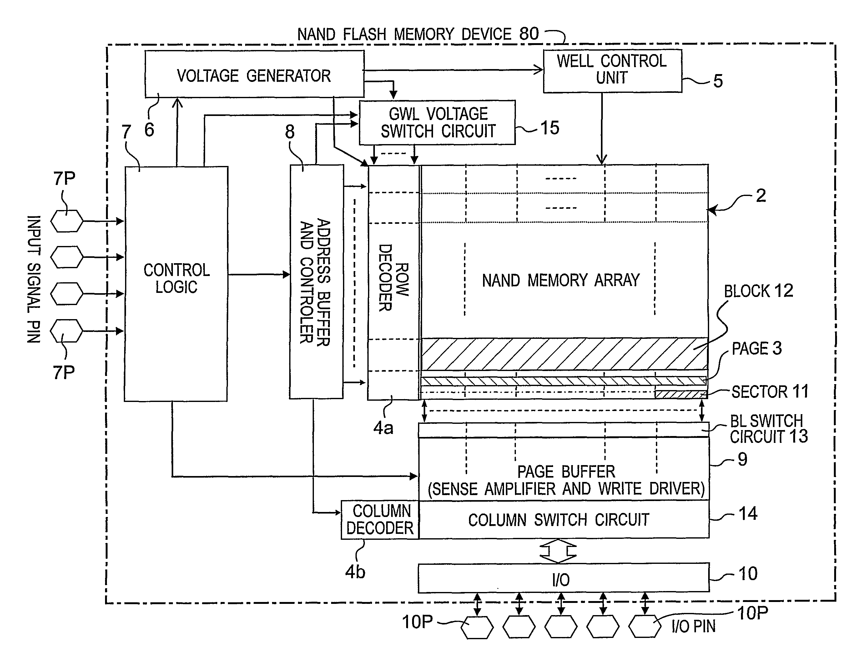
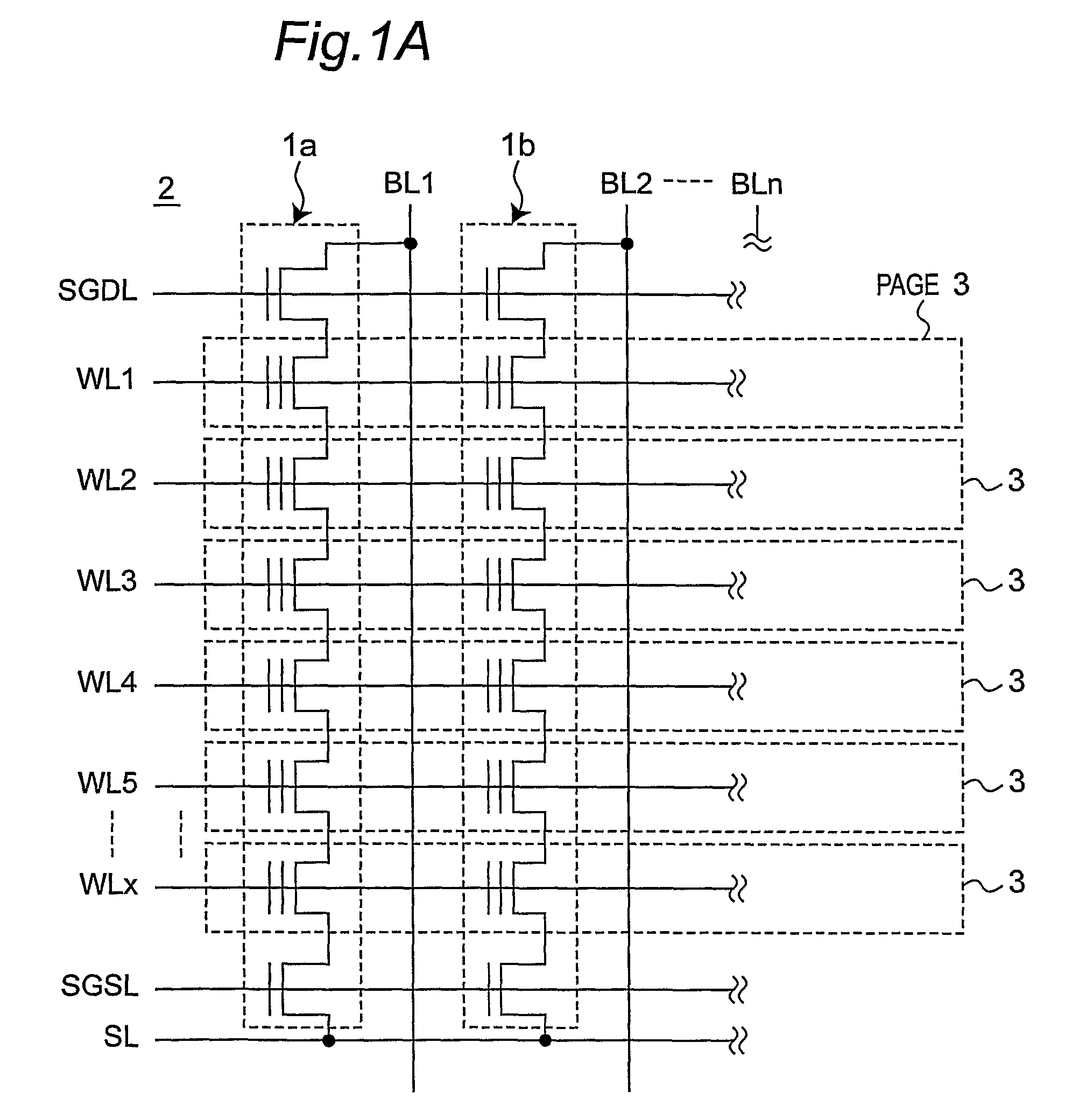
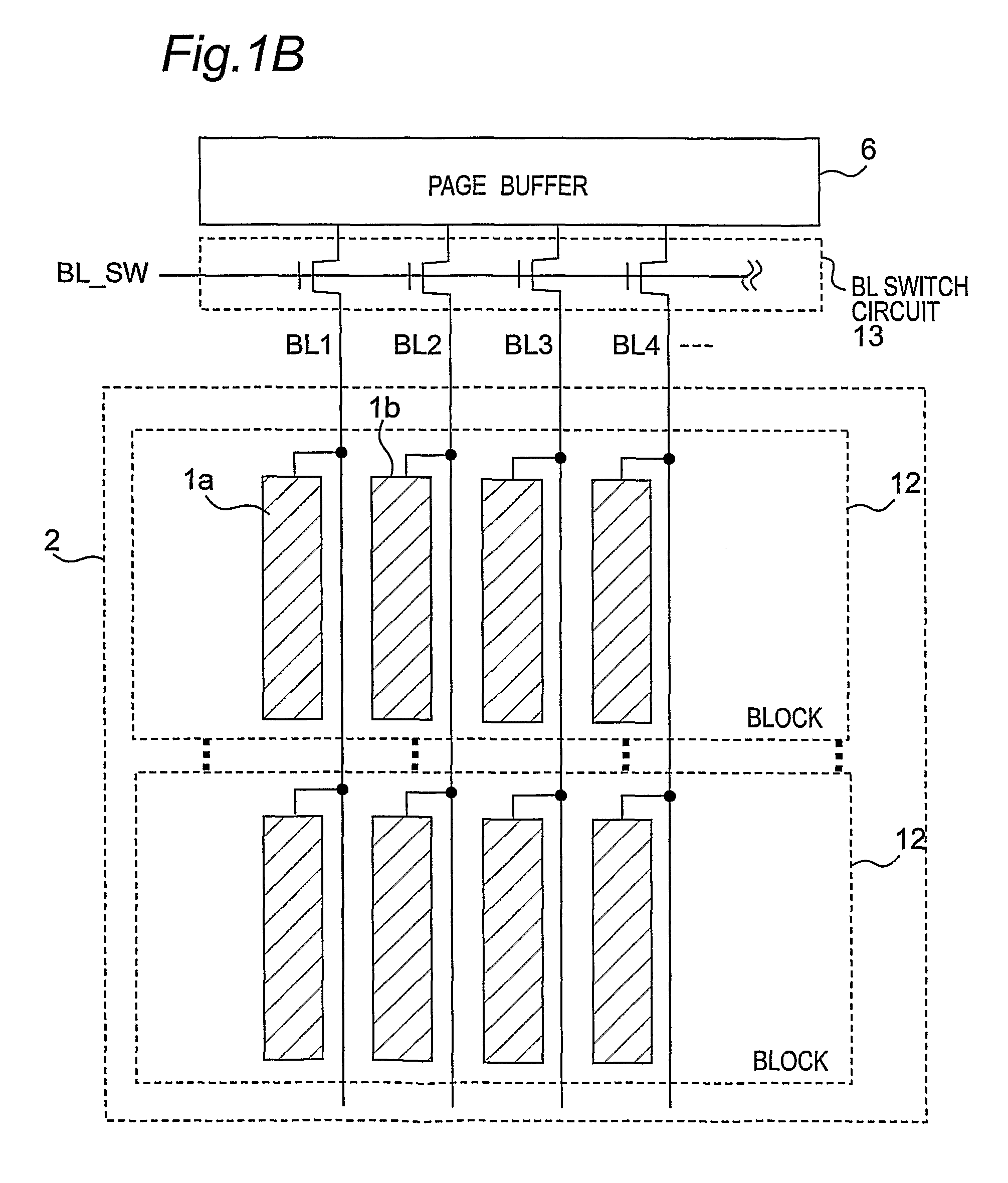
[0168]FIG. 1A is a schematic circuit diagram showing a configuration of a NAND flash memory array 2 of a first preferred embodiment according to the present invention, FIG. 1B is a schematic block diagram of a configuration of the NAND flash memory array 2 of FIG. 1 and peripheral circuits thereof, and FIG. 2 is a longitudinal cross sectional view along a cell string of a configuration of the NAND flash memory array 2 of FIGS. 1A and 1B.

[0169]Referring to FIG. 1, the NAND flash memory array 2 includes a plurality of word lines WL1 to WLx, two selected gate lines SGSL and SGDL, a plurality of bit lines BL1 to BLn, and a source line SL, where x and n are each an integer equal to or larger than two. The parts of the word lines WL1 to WLx spanning over the active area correspond to memory cells. The cell strings composed of the memory cells are disposed below the bit lines BL1 to BLn, where the cell string 1a is connected to the bit line BL1, and the cell string 1b is connected to the b...

second preferred embodiment

[0199]Our proposed programming scheme using the negative gate voltage can be done by the row decoder 4a which will be described below.

[0200]FIG. 20A is a schematic circuit diagram showing a configuration of a high voltage level shifter (referred to as an HVLS hereinafter) 21 and a word line driver (referred to as a WL driver hereinafter) 22 of the row decoder 4a according to a second preferred embodiment of the present invention, FIG. 20B is a schematic circuit diagram showing a configuration of a high voltage level shifter (referred to as an HVMVLS hereinafter) 24 and the WL driver 22 of the row decoder 4a according to the second preferred embodiment of the present invention, and FIG. 21A is a timing chart showing a programming scheme of the second preferred embodiment based on the timing chart of FIG. 12 of the first preferred embodiment. Namely, FIG. 21A shows a programming sequence according to the second preferred embodiment of the present invention, based on the timing chart o...

third preferred embodiment

[0233]The leveraged benefit for file system application brought by this programming method will be described hereinafter.

[0234]FIG. 34A is a graph showing a threshold voltage Vth shift by the program disturb after a partial programming according to a prior art, and FIG. 34B is a graph showing a threshold voltage Vth shift by the program disturb after a partial programming according to the preferred embodiments of the present invention. FIG. 34C is a schematic block diagram showing a unit of partial programming in the page 3 which is used for FIGS. 34A and 34B, and FIG. 34D is a schematic block diagram showing a programming sequence for a storage unit such as a solid-state drive (SSD) which is used for FIG. 34B.

[0235]Although the program disturb occurs seriously in the conventional programming scheme as shown in FIG. 34A, no threshold voltage (Vth) shift is seen after over programming at the same page in our proposed programming method as shown in FIG. 34B, where the program disturb ...


PUM


Abstract

In a programming method for a NAND flash memory device, a self-boosting scheme is used to eliminate excess electrons in the channel of an inhibit cell string that would otherwise cause programming disturb. The elimination is enabled by applying a negative voltage to word lines connected to the inhibit cell string before boosting the channel, and this leads to bringing high program immunity. A row decoder circuitry to achieve the programming operation and a file system architecture based on the programming scheme to improve the efficiency of file management are also described.

Description

TECHNICAL FIELD[0001]The present invention relates to a programming method for a NAND flash memory device including a NAND flash memory array, and to a NAND flash memory device including a NAND flash memory array.BACKGROUND ART[0002]NAND flash memories have been developed for high density storage application, such as picture cards for digital cameras, memory of MP players, and universal serial bus (USB) memories. In particular, a cellular phone system and personal digital assistants (PDA) have shown rapid growth to expand its market segment. Further, its application has been extended to PC storage use as a solid-state drive (referred to as an SSD hereinafter), which is an alternative of a hard disk drive (HDD), and is the most promising market domain for the NAND flash memory in the future. However, as the scaling technology for finer pattern in the semiconductor memories is further developed, the NAND flash memories face such a physical limitation as in terms of the cell operabilit...

Claims


Application Information

Patent Timeline
Patent Type & Authority Patents(United States)
IPC IPC(8): G11C11/34
CPCG11C16/10G11C16/3418G11C16/3427H01L27/11526G11C16/0483G11C16/08G11C16/102H01L27/11524H10B41/40H10B41/35
Inventor MIIDA, TAKASHISHIROTA, RIICHIROARAKAWA, HIDEKIYANG, CHING SUNGLIN, TZUNG LING
Owner POWERCHIP SEMICON MFG CORP
Why Eureka
Try Eureka