Solid-state imaging device, drive method thereof and electronic apparatus

a solid-state imaging and drive method technology, applied in the direction of radioation control devices, television systems, television system scanning details, etc., can solve the problems of reduced saturation charge amount (qs) per unit, disadvantageous configuration for pixel characteristics, white defects, etc., to improve saturation charge amount (qs), increase saturation charge amount (qs), and improve saturation charge amount (qs) and sensitivity

Active Publication Date: 2013-12-24
SONY CORP
View PDF64 Cites 25 Cited by
  • Summary
  • Abstract
  • Description
  • Claims
  • Application Information

AI Technical Summary

Benefits of technology

[0034]It is desirable to provide a solid-state imaging device and an electronic apparatus using the solid-state imaging device in which increase of the saturation charge amount (Qs) and improvement of sensitivity can be realized as well as having high transfer efficiency of signal charges.
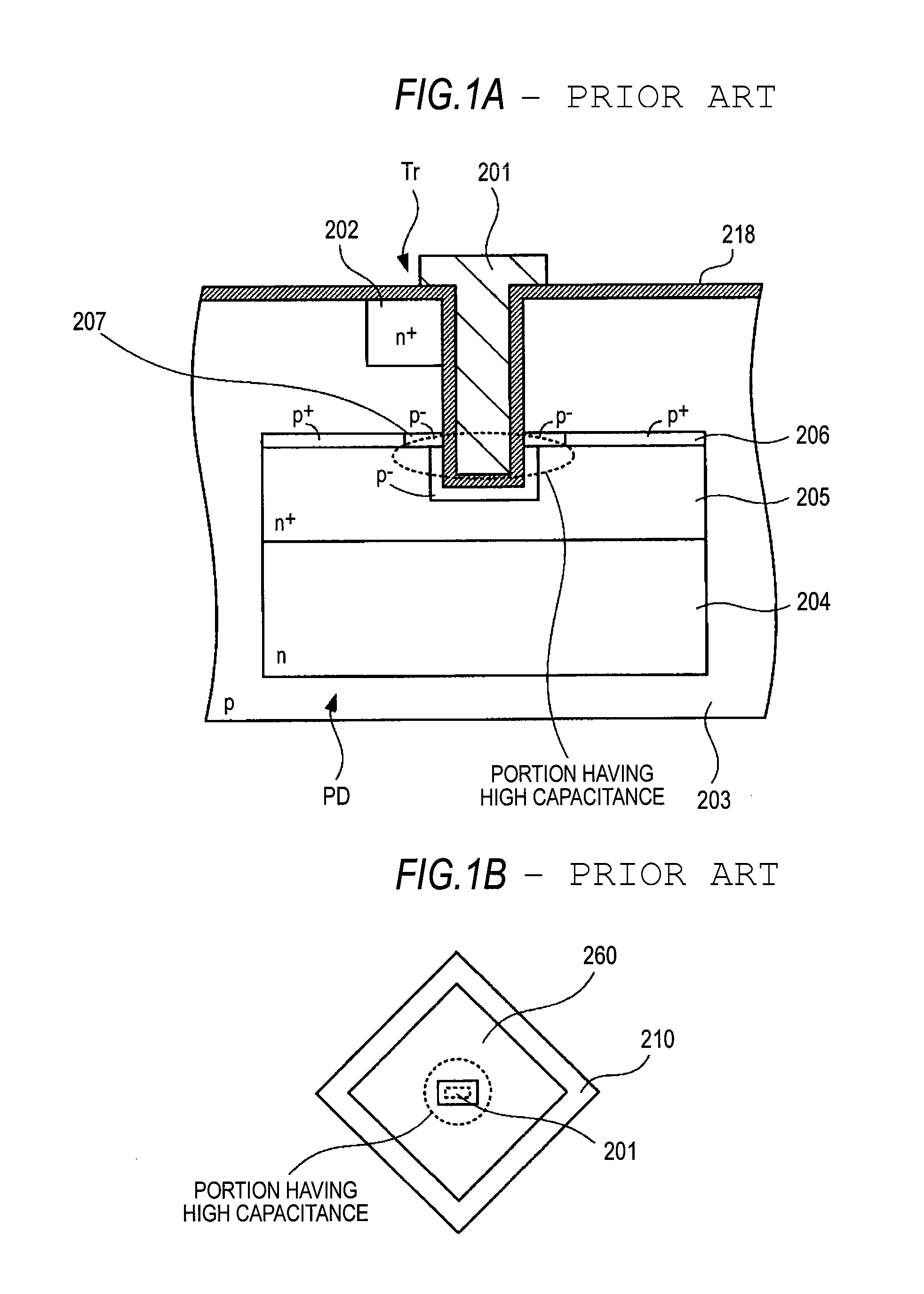
[0035]In the above solid-state imaging device 1111, the vertical transfer transistor Tr1 is arranged in the center of the pixel to thereby allow distances between the periphery of the photodiode PD and the transfer gate electrode 1116 are the same and make the complete transfer of signal charges easy. However, the transfer gate electrode 1116 may inhibit formation of the photodiode PD. Therefore, it is difficult to allow a portion of the transfer gate electrode 1116 to be formed as the photodiode PD, which reduces the saturation charge amount (Qs) per a unit area, as a result, a configuration will be disadvantageous for pixel characteristics.

Problems solved by technology

Therefore, it is difficult to allow a portion of the transfer gate electrode 1116 to be formed as the photodiode PD, which reduces the saturation charge amount (Qs) per a unit area, as a result, a configuration will be disadvantageous for pixel characteristics.
However, in the configuration, n+region 1113A exists below the transfer gate electrode in the state of touching the electrode, therefore, there are fears that white defects caused by dark current due to GIDL (Gate Induced Drain Leakage) occur and that pixel characteristics are reduced.
However, when the region 1122 is“p−”, it is difficult to secure a transfer path actually.

Method used


Image

  • Solid-state imaging device, drive method thereof and electronic apparatus
  • Solid-state imaging device, drive method thereof and electronic apparatus
  • Solid-state imaging device, drive method thereof and electronic apparatus

Examples


embodiment 1

Example Including Two Vertical Gate Electrodes

[0196]FIG. 6 shows a schematic planar configuration of a solid-state imaging device according to Embodiment 1 of the invention, and FIG. 7 shows a schematic cross-sectional configuration taken along A-A line of FIG. 6. FIG. 6 and FIG. 7 are a plan view and a cross-sectional view of a relevant part included in one pixel. As shown in FIG. 6 and FIG. 7, the solid-state imaging device includes a photodiode PD and a charge readout transistor Tr formed in a semiconductor substrate 13. The charge readout transistor Tr includes two vertical gate electrodes 12a, 12b formed in a peripheral portion of the photodiode PD and a floating diffusion region 11 formed at a corner portion of a photodiode region 60 toward an outside region. In the present embodiment, a case in which a first conductive type is a p-type and a second conductive type is an n-type will be explained.

[0197]The semiconductor substrate 13 is made of a p-type silicon substrate.

[0198]T...

embodiment 2

Example Including Two Vertical Gate Electrodes

[0213]FIG. 9 shows a schematic planar configuration of a solid-state imaging device according to Embodiment 2 of the invention, and FIG. 10 shows a cross-sectional configuration taken along B-B line. The present embodiment differs from the Embodiment 1 in a position in which the floating diffusion region 11 is formed. In FIG. 9 and FIG. 10, same symbols are given to portions corresponding to FIG. 6 and FIG. 7, and the repeated explanation is omitted.

[0214]In the solid-state imaging device of the embodiment, the floating diffusion region 11 is formed on the surface side of the semiconductor substrate 13 from the corner portion of the photodiode region 60 sandwiched by the vertical gate electrodes 12a, 12b toward the inside of the photodiode region 60. The floating diffusion region 11 is shared between the two vertical gate electrodes 12a, 12b. In the embodiment, the floating diffusion region 11 is formed so as to touch the vertical gate e...

embodiment 3

Example Including Two Vertical Gate Electrodes and a Planar Gate Electrode

[0217]FIG. 11 shows a schematic planar configuration of a solid-state imaging device according to Embodiment 3 of the invention, and FIG. 12 shows a cross-sectional configuration taken along C-C line of FIG. 11. In FIG. 11 and FIG. 12, same symbols are given to portions corresponding to FIG. 6 and FIG. 7 and the repeated explanation is omitted.

[0218]In the solid-state imaging device of the present embodiment, the charge readout transistor Tr included in one pixel includes a planar gate electrode 19, the vertical gate electrodes 12a, 12b and the floating diffusion region 11.

[0219]The two vertical gate electrodes 12a, 12b are formed at an outer peripheral portion of the photodiode region 60 respectively along two edges forming a corner portion of the photodiode region 60. On an upper surface of the semiconductor substrate 13 positioned at the corner portion of the photodiode region 60 sandwiched by the vertical ...


PUM


Abstract

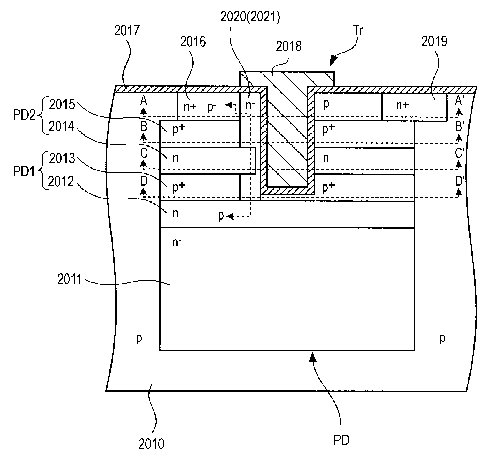
A solid-state imaging device includes: plural photodiodes formed in different depths in a unit pixel area of a substrate; and plural vertical transistors formed in the depth direction from one face side of the substrate so that gate portions for reading signal charges obtained by photoelectric conversion in the plural photodiodes are formed in depths corresponding to the respective photodiodes.

Description

BACKGROUND OF THE INVENTION[0001]1. Field of the Invention[0002]The invention relates to a solid-state imaging device including plural photodiodes in a unit pixel area, a drive method thereof and an electronic apparatus using the solid-state imaging device.[0003]2. Description of the Related Art[0004]Color separation in a CCD image sensor or a CMOS image sensor as a solid-state imaging device is realized by mainly using color filters. In the image sensor using color filters, a color filter of one kind is mounted with respect to one pixel, and three pixel circuits principally having color filters of red, green and blue are arranged so as to be adjacent to one another. Accordingly, light which can be received in one pixel is only one color corresponding to the color filter in a narrow sense. Therefore, in the image sensor using color filters, colors are generated by using information of light incident on adjacent pixels on which color filters of different colors are mounted.[0005]Ther...

Claims


Application Information

Patent Timeline
Patent Type & Authority Patents(United States)
IPC IPC(8): H04N5/335
CPCH01L27/14603H01L27/14647H01L27/14641H01L27/14887H01L27/1464H01L27/14625H01L27/14656H01L27/146
Inventor WATANABE, TAIICHIROYAMADA, AKIHIROKIDO, HIDEOSAITO, HIROMASAMABUCHI, KEIJIOHGISHI, YUKO
Owner SONY CORP
Why Eureka
Try Eureka