
Photomultiplier tube optimized for surface inspection in the ultraviolet

a technology of surface inspection and photomultiplier tube, which is applied in the field of photomultiplier tube, can solve the problems of unsuitable wafer inspection for the photomultiplier tube found in the art, and achieve the effects of low noise, high efficiency and low gain

Active Publication Date: 2014-01-14
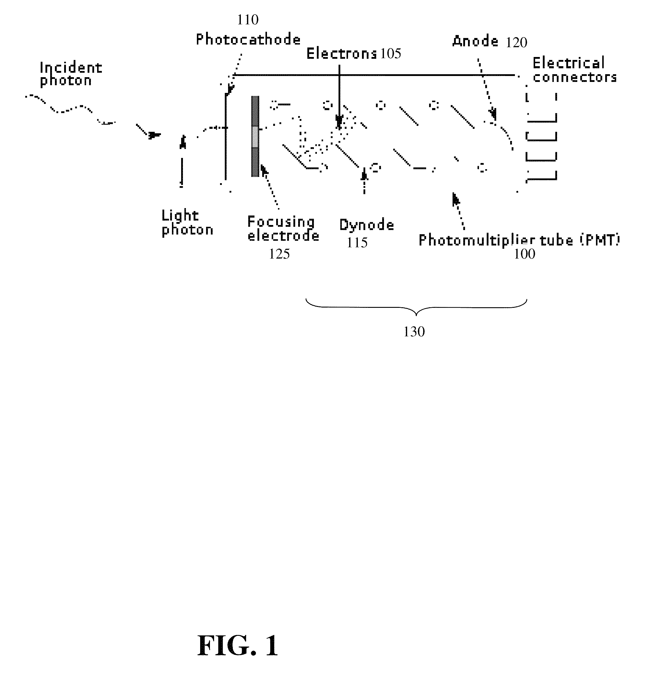
KLA TENCOR TECH CORP
View PDF11 Cites 41 Cited by
  • Summary
  • Abstract
  • Description
  • Claims
  • Application Information

AI Technical Summary

Benefits of technology

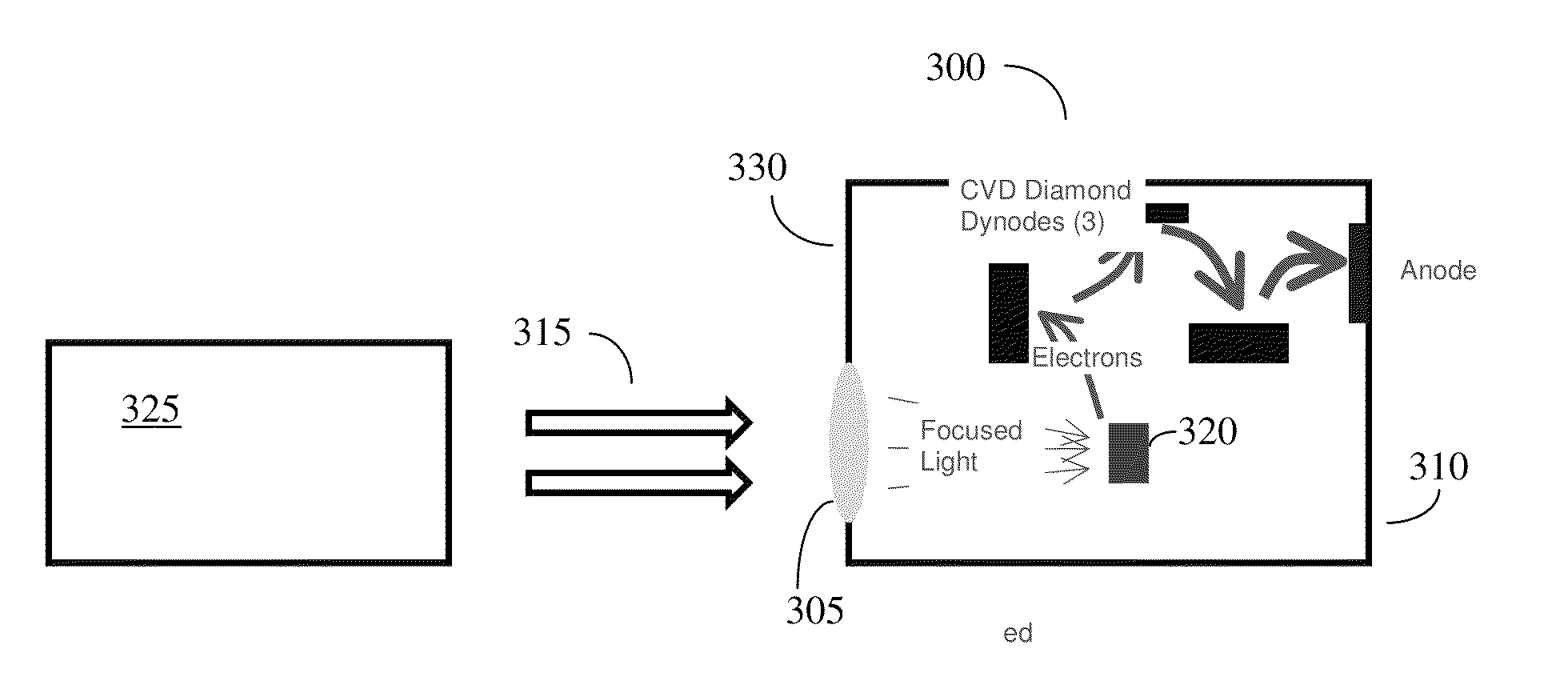
The patent describes a high-efficiency, low-noise, and low-gain PMT designed for surface inspection systems. The PMT is designed to be tuned to a specific wavelength that maximizes QE. It uses a combination of small dynodes with high secondary electron gain to reduce excess noise and improve S / N. The lower overall PMT gain ensures compatibility with surface inspection systems.

Problems solved by technology

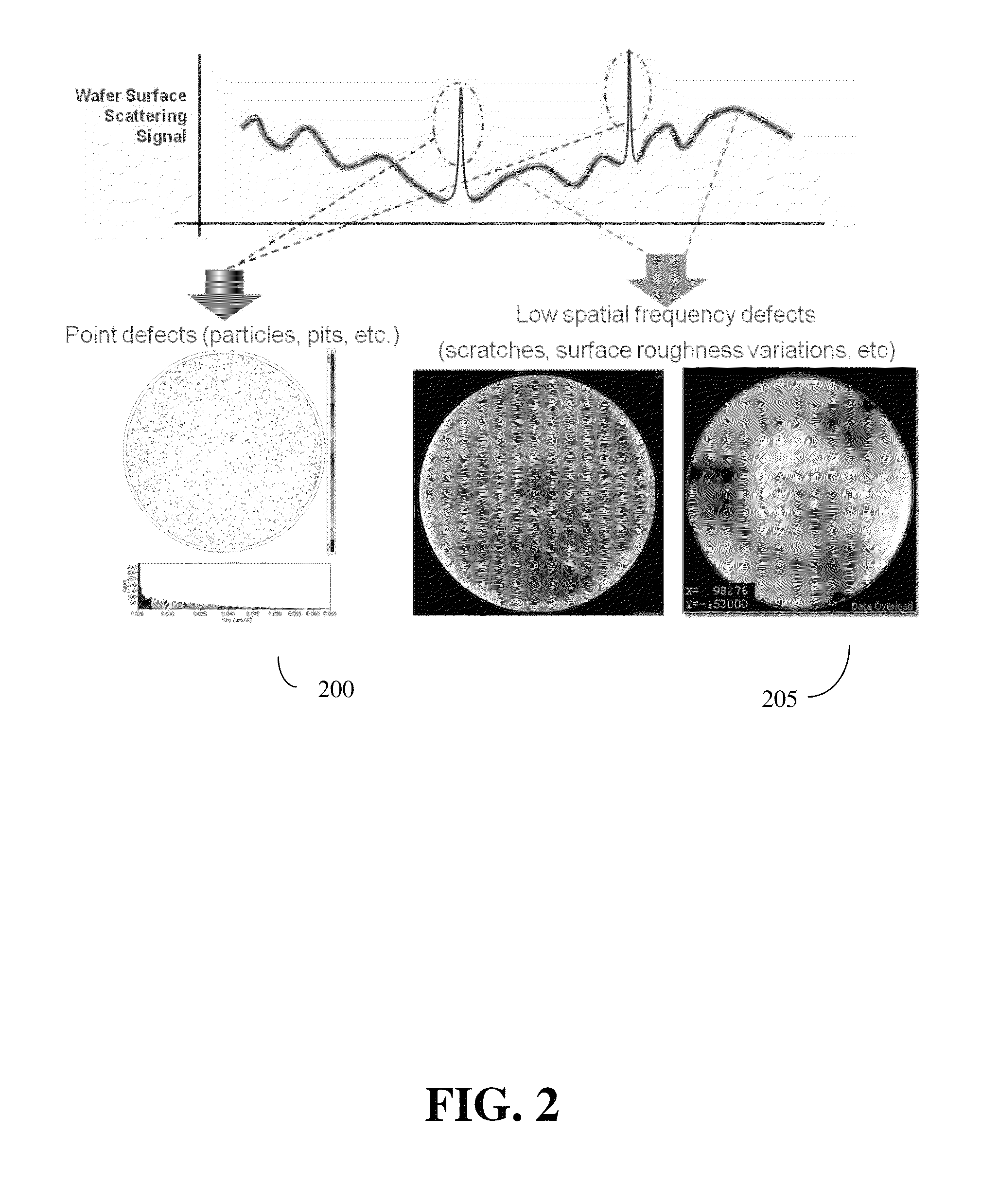
However, as will be described, the desirable characteristics of photomultiplier tubes used in wafer inspection applications differ greatly from those of typical photomultiplier applications, and therefore photomultiplier tubes found in the art are ill suited to wafer inspection.

Method used


Image

  • Photomultiplier tube optimized for surface inspection in the ultraviolet
  • Photomultiplier tube optimized for surface inspection in the ultraviolet
  • Photomultiplier tube optimized for surface inspection in the ultraviolet

Examples


Embodiment Construction

[0013]In contrast to photomultiplier requirements for typical applications, the requirements for photomultiplier tubes used in unpatterned surface inspection are quite different. First, a typical surface inspection system operates at a single ultraviolet wavelength, and therefore the photomultiplier tube need not be sensitive to any other wavelengths; preferably, a PMT will be particularly tuned to the specific UV wavelength of the inspection system. Secondly, the electron gain requirements of a PMT incorporated in a surface inspection system are relatively modest, between about 50 and 50,000 (at least an order of magnitude less than conventional PMT's). A PMT gain in the range between about 50 and 50,000 will be hereinafter referred to as “low gain”. The gain requirements are fairly low because the levels of incident light are relatively high, up to tens of nanowatts. Many other PMT applications, such as high energy physics or medical instrumentations, have background light levels ...


PUM


Abstract

Disclosed herein is a PhotoMultiplier Tube (PMT) designed for use with a surface inspection system such as the Surfscan system, which operates at 266 nm wavelength. The inventive PMT is high efficiency, low noise, and low gain, a combination of features that is specific to the application and contrary to the features of PMT's in the art. The inventive PMT is designed to be tuned to a specific narrow band wavelength of incident light, thereby optimizing the QE at that wavelength. It is further designed to combine a small number of dynodes each having substantially higher secondary electron gain than typical dynodes. By designing the PMT in this way, the excess noise factor is dramatically reduced, yielding a much improved S / N, while still maintaining the overall PMT gain in the lower range suitable for use in a surface inspection system.

Description

CROSS REFERENCE TO RELATED APPLICATION[0001]This application is related to U.S. Provisional application No. 61 / 254,977, filed Oct. 26, 2009, and claims priority therefrom.FIELD OF THE INVENTION[0002]This invention relates to inspection of wafers for integrated circuits, and in particular to the development of a photomultiplier tube designed for optimum performance with a wafer inspection system for unpatterned wafers.BACKGROUND[0003]Wafer inspection systems for inspecting bare or unpatterned wafers are important in many ways, such as qualifying bare wafers, detecting surface anomalies, inspecting rough films, etc. U.S. Pat. No. 6,201,601, issued Mar. 13, 2001, describes a wafer inspection system for bare or unpatterned wafers, made by KLA-Tencor, Inc., generally referred to as the SurfScan system. U.S. Pat. No. 6,201,601 is hereby incorporated by reference in its entirety.[0004]Detectors utilized in wafer inspection systems such as Surfscan include photomultiplier tubes (PMT's). How...

Claims


Application Information

Patent Timeline
IPC IPC(8): H01J40/06H01J40/00H01J40/14
CPCH01J43/28H01J40/14H01J40/06H01J40/00
Inventor BIELLAK, STEPHENKAVALDJIEV, DANIELFRIEDMAN, STUART
Owner KLA TENCOR TECH CORP
Learn More