

Method and system of heterogeneous substrate bonding for photonic integration
a heterogeneous substrate and photonic integration technology, applied in semiconductor lasers, semiconductor/solid-state device details, instruments, etc., can solve the problem that silicon is not a direct bandgap material, and achieve good mechanical strength, good electrical conductivity, and sufficient compliance
- Summary
- Abstract
- Description
- Claims
- Application Information
AI Technical Summary
Benefits of technology
Problems solved by technology
Method used
Image

Examples
Embodiment Construction
[0018]Embodiments of the present invention relate to an apparatus and method that preferably uses a bonding stress for wafer bonding and utilizes an intermediate layer to facilitate the transition from silicon and the like to another material for optical coupling as well as electron transport. Embodiments of the present invention preferably incorporate low stress, low temperature wafer bonding known in the industry and preferably comprise a thin film intermediate layer for optical coupling as well electron transport.
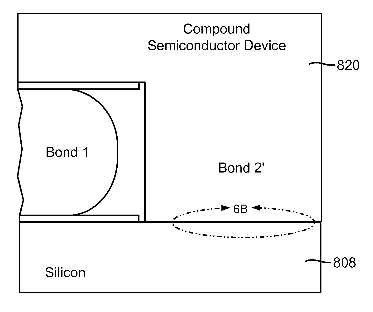
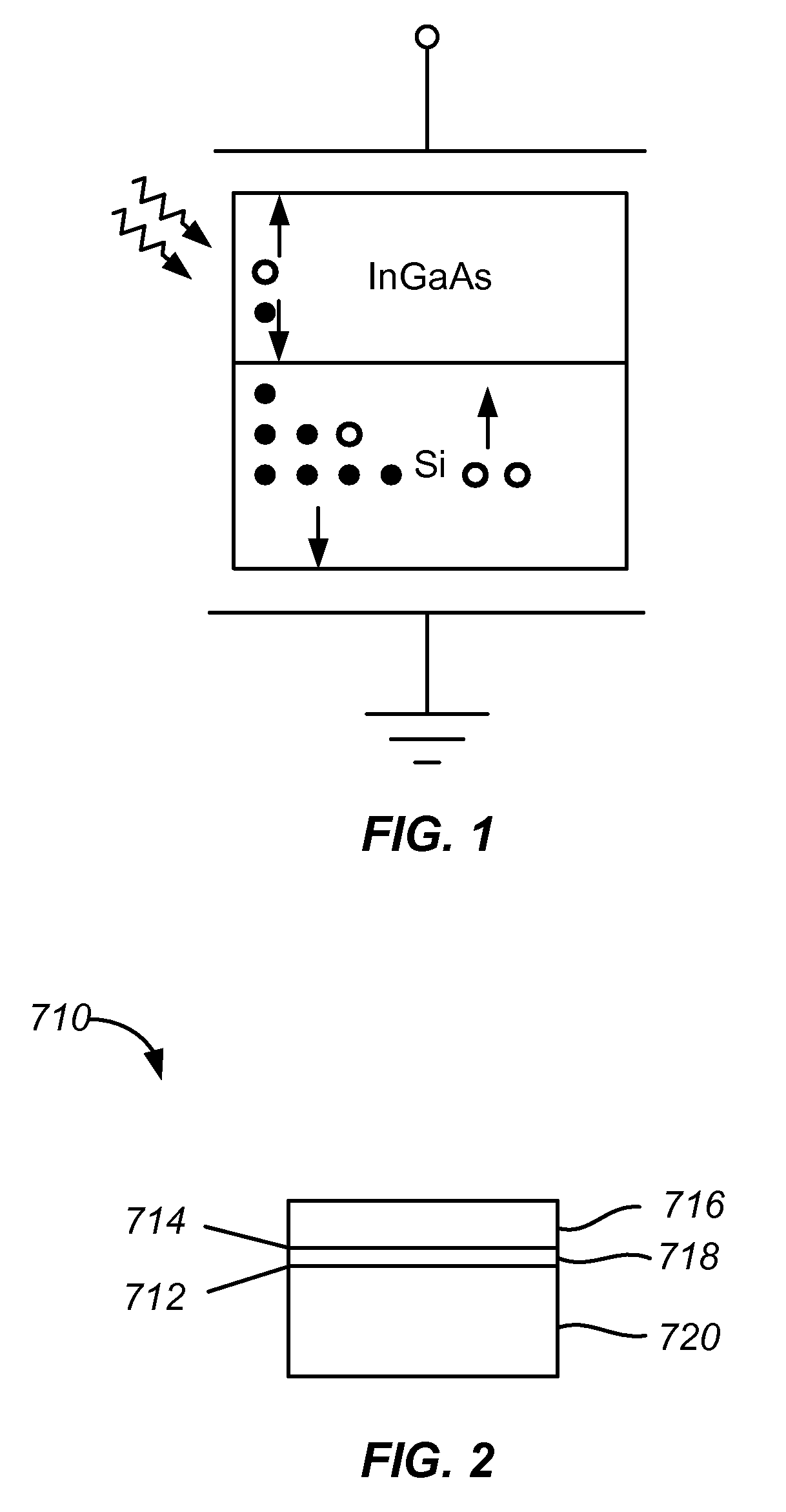
[0019]FIG. 1 illustrates an example of a photodiode with a low stress bond between a III-V substrate and a silicon substrate. FIG. 2 illustrates a bonded structure according to an embodiment of the present invention. As illustrated in FIG. 2, two interfaces 712 and 714 are provided. First interface 712 is positioned between a silicon substrate 720 and an intermediate layer 718. Second interface 714 is located between intermediate layer 718 and a second semiconductor laye...
PUM
| Property | Measurement | Unit |
|---|---|---|
| temperatures | aaaaa | aaaaa |
| temperature | aaaaa | aaaaa |
| temperature | aaaaa | aaaaa |
Abstract
Description
Claims
Application Information