Semiconductor structure and method for manufacturing the same

a technology of semiconductor structure and semiconductor structure, which is applied in the direction of semiconductor/solid-state device details, semiconductor devices, electrical apparatus, etc., can solve the problems of affecting the performance of transistors, so as to reduce contact resistance and low resistance, and achieve the effect of reducing the contact resistan

Active Publication Date: 2014-02-04
INST OF MICROELECTRONICS CHINESE ACAD OF SCI
View PDF8 Cites 10 Cited by
  • Summary
  • Abstract
  • Description
  • Claims
  • Application Information

AI Technical Summary

Benefits of technology

[0008]The present invention aims to provide a semiconductor structure and a method for manufacturing the same, which are favorable for reducing the contact resistance between source / drain regions and a contact layer (e.g. a metal silicide layer).
[0024]As compared to the prior art, the present invention exhibits following advantages:
[0025]1) the area of a region covered by a contact layer on the surface of the source / drain regions may be increased by way of forming a first contact layer on the surface of the source / drain regions and forming a second contact layer on the first contact layer exposed by through holes or on the first contact layer and a portion of the surface of the source / drain regions, and it is thence favorable for reducing the contact resistance between the source / drain regions and the contact layer (e.g. a metal silicide layer);
[0026]2) the first contact layer exhibits thermal stability under the temperature required for annealing at formation of a gate stack structure, thus it is able to maintain a low resistance under a rather high temperature for annealing (e.g. 850° C.), therefore, the subsequent processes may be performed under a high temperature without impeding performance of the semiconductor structure;
[0027]3) the formation of the first contact layer is favorable for restraining generation of piping defect so as to reduce occurrence of short circuits in the semiconductor structure.

Problems solved by technology

When the gate dielectric layer of a MOSFET is made of a high-k dielectric material, the gate drain current shall be effectively reduced; however, as a high-k gate dielectric layer is formed at first, the molecular structure of the high-k gate dielectric layer probably have defects.
However, a metal silicide layer in the transistor cannot endure the high temperature required for annealing the high-k dielectric layer, wherein the structure of the metal silicide layer is prone to change under the high temperature, such that the resistivity of the metal silicide layer increases, which thereby impedes performance of the transistor.
However, aforesaid method though is able to protect the metal silicide layer from damage arising from annealing of the high-k dielectric layer, limitations of the method lies in that the metal silicide layer is formed nowhere but between the contact trench and the source / drain regions, thus the area of the region covered by metal silicide on the surface of the source / drain regions is limited, thus the contact resistance between the source / drain regions and the metal silicide layer of the transistor cannot be reduced adequately.

Method used


Image

  • Semiconductor structure and method for manufacturing the same
  • Semiconductor structure and method for manufacturing the same
  • Semiconductor structure and method for manufacturing the same

Examples


Embodiment Construction

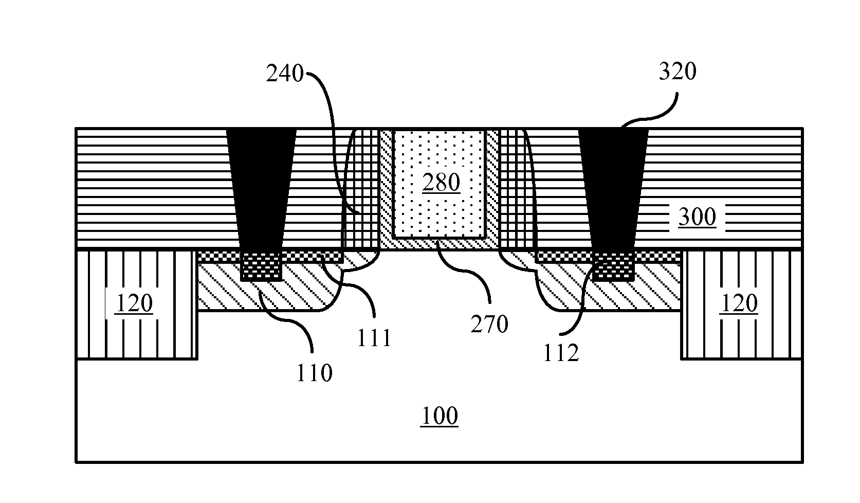
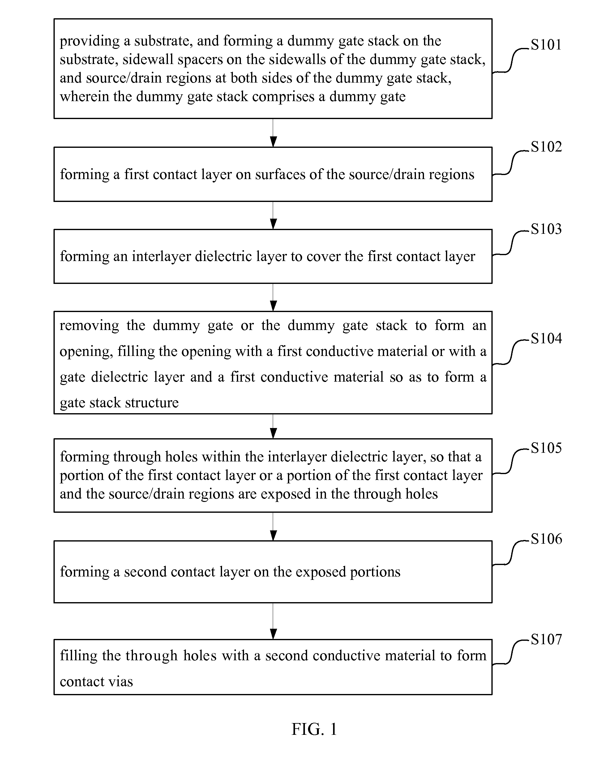
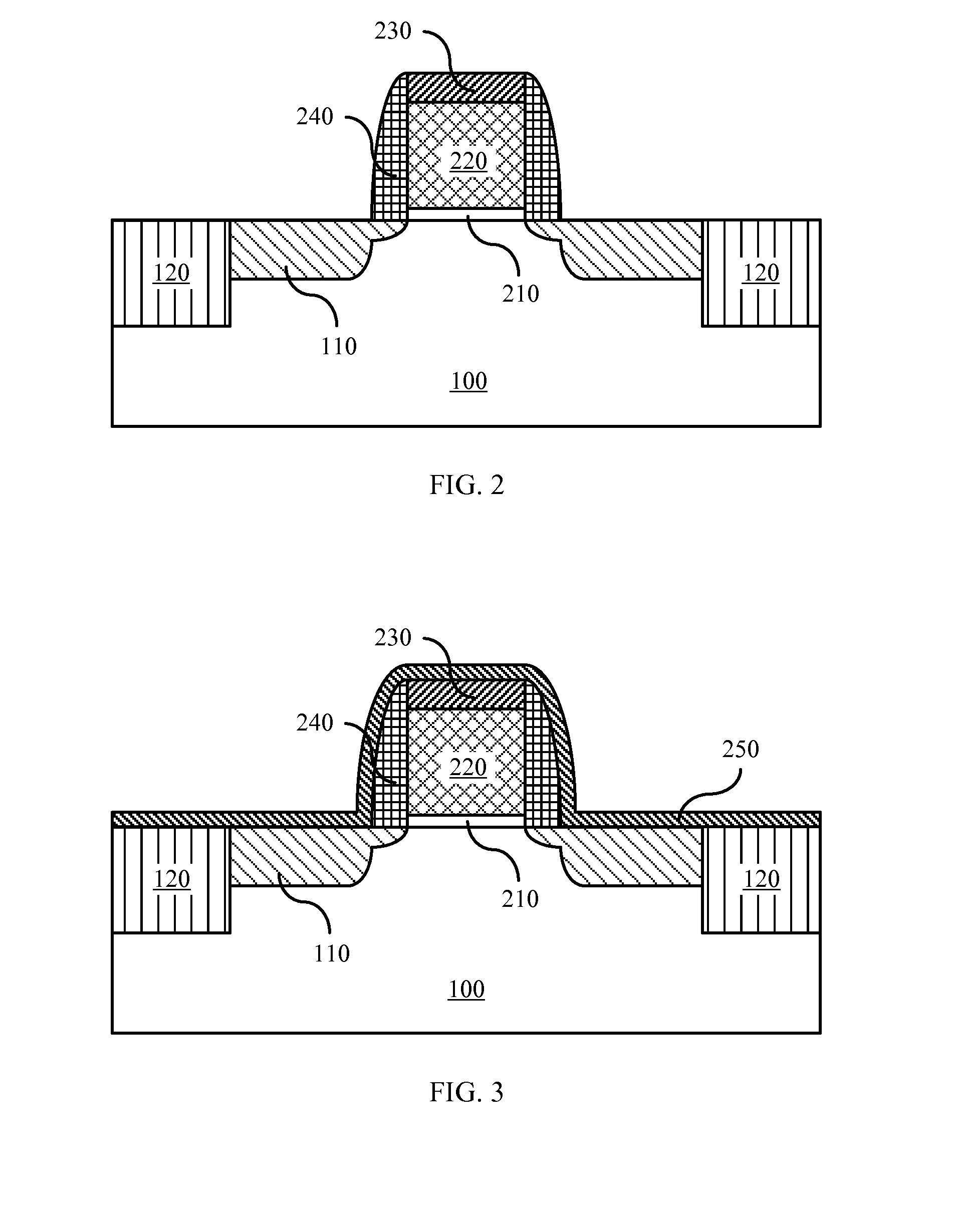
[0034]Described below in detail are preferred embodiments of the present invention, examples of which are illustrated in the drawings. The embodiments described below with reference to the drawings are merely illustrative, and are provided for explaining the present invention only, thus should not be interpreted as limitations to the present invention.

[0035]Various embodiments or examples are provided here below to implement the different structures of the present invention. To simplify the disclosure of the present invention, description of the components and arrangements of specific examples is given below. Of course, they are only illustrative and not limiting the present invention. Moreover, in the present invention, reference numbers and / or letters may be repeated in different embodiments. Such repetition is for the purposes of simplification and clearness, and does not denote the relationship between respective embodiments and / or arrangements being discussed. Furthermore, the ...


PUM


Abstract

The present invention provides a method for manufacturing a semiconductor structure. The method can effectively reduce the contact resistance between source / drain regions and a contact layer by forming two contact layers of different thickness on the surfaces of the source / drain regions. Further, the present invention provides a semiconductor structure, which has reduced the contact resistance.

Description

CROSS REFERENCE TO RELATED APPLICATION[0001]This application is a National Phase application of, and claims priority to, PCT Application No. PCT / CN2011 / 071350, filed on Feb. 27, 2011, entitled “SEMICONDUCTOR STRUCTURE AND METHOD FOR MANUFACTURING THE SAME”, which claimed priority to Chinese Application No. 201010572608.3, filed on Dec. 3, 2010. Both the PCT Application and Chinese Application are incorporated herein by reference in their entireties.FIELD OF THE INVENTION[0002]The present invention relates generally to the field of semiconductors and semiconductor manufacturing, and more particularly, to a semiconductor structure and methods for manufacturing the same.BACKGROUND OF THE INVENTION[0003]The Metal-Oxide-Semiconductor Field-Effect Transistor (MOSFET) is a kind of transistor that is widely applied in digital circuits and analog circuits. When the gate dielectric layer of a MOSFET is made of a high-k dielectric material, the gate drain current shall be effectively reduced; ...

Claims


Application Information

Patent Timeline
Patent Type & Authority Patents(United States)
IPC IPC(8): H01L29/94H01L29/78
CPCH01L29/7833H01L29/49H01L21/76814H01L21/28518H01L29/66545H01L29/517H01L21/28185H01L29/66492
Inventor YIN, HAIZHOULUO, JUNZHU, HUILONGLUO, ZHIJIONG
Owner INST OF MICROELECTRONICS CHINESE ACAD OF SCI
Why Eureka
Try Eureka