Sapphire wafer dividing method

a technology of sapphire and dividing method, which is applied in the direction of manufacturing tools, laser beam welding apparatus, welding/soldering/cutting articles, etc., can solve the problem of inefficient extraction of light from sapphire substrate, achieve easy incident, suppress the preservation of reflective angle, and improve the luminance of each light emitting devi

Active Publication Date: 2014-03-18
DISCO CORP
View PDF6 Cites 3 Cited by
  • Summary
  • Abstract
  • Description
  • Claims
  • Application Information

AI Technical Summary

Benefits of technology

[0007]It is therefore an object of the present invention to provide a sapphire wafer dividing method which can improve the luminance of the light emitting device formed by dividing a sapphire wafer.
[0009]With this configuration, the cut grooves are formed on the back side of the sapphire wafer along the division lines in the chamfering and dividing step, thereby chamfering the corners of the back side of each light emitting device divided from the sapphire wafer. By performing this chamfering, a polyhedral surface is formed on the back side of each light emitting device, so that the light reflected in the device is easily incident on the polyhedral surface at an angle less than or equal to the critical angle. Accordingly, the light emitted from the light emitting layer of each device can be easily emerged to the outside, thereby improving the luminance of each light emitting device. The chamfering to be performed in the present invention is not limited to forming the corners of each light emitting device into slant surfaces, but includes forming the corners of each light emitting device into any shape such as curved surfaces capable of suppressing the preservation of a reflective angle. Further, the cut grooves are formed after forming the modified layers inside the sapphire wafer. Accordingly, an external force is applied to the modified layers in forming the cut grooves, so that the sapphire wafer is divided along the modified layers as a division start point. Thus, the division of the sapphire wafer can be performed simultaneously with the formation of the cut grooves on the sapphire wafer, so that the number of steps can be reduced to improve the working efficiency.
[0010]According to the present invention, the cut grooves are formed on the sapphire wafer along the division lines to divide the sapphire wafer into the individual light emitting devices along the cut grooves, so that the light emitted from the light emitting layer of each light emitting device can be easily emerged to the outside to improve the luminance. Further, the cut grooves are formed after forming the modified layers inside the sapphire wafer, so that the division of the sapphire wafer can be performed simultaneously with the formation of the cut grooves on the sapphire wafer.

Problems solved by technology

However, since the refractive index of sapphire is remarkably larger than that of air, there is a problem such that the light is not efficiently emerged from the sapphire substrate.

Method used


Image

  • Sapphire wafer dividing method
  • Sapphire wafer dividing method
  • Sapphire wafer dividing method

Examples


Embodiment Construction

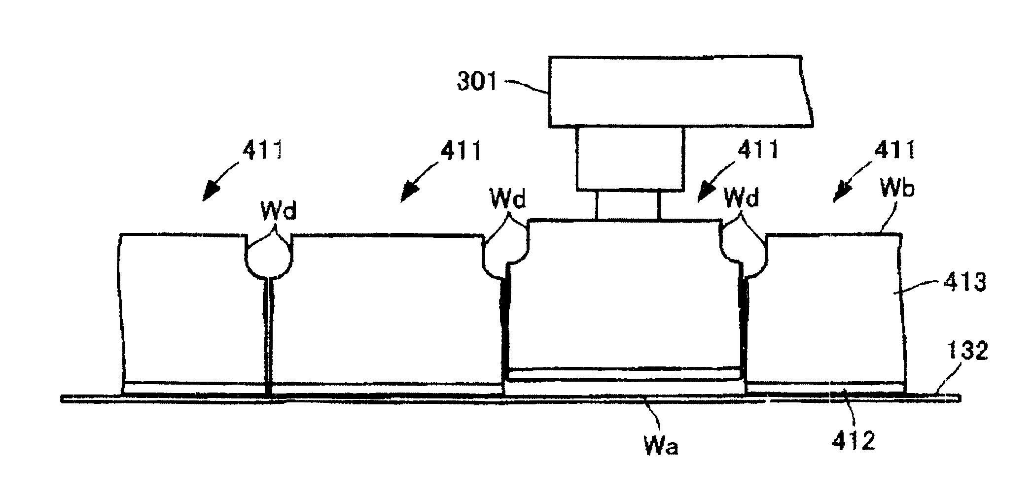
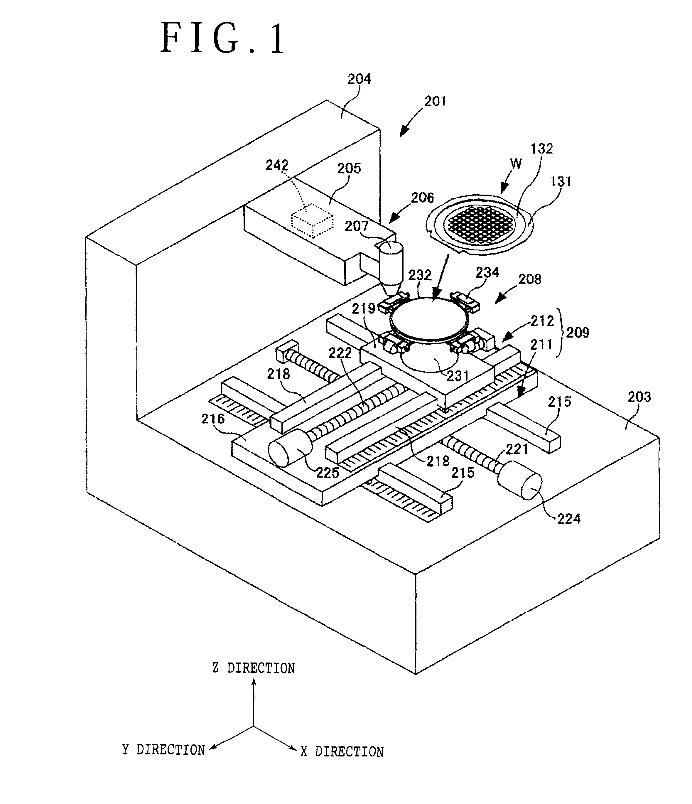
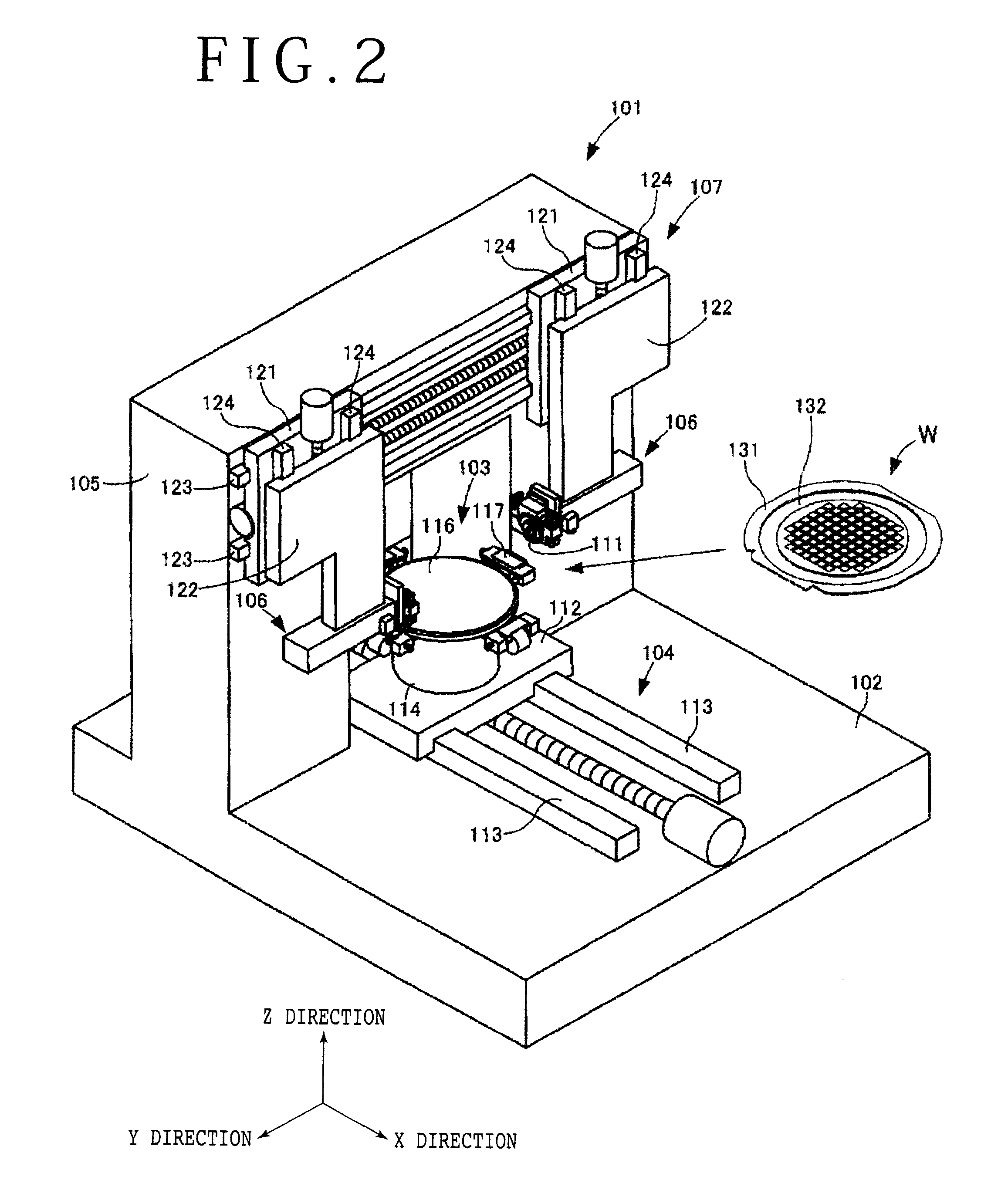
[0018]The division of a sapphire wafer using a dividing method according to a preferred embodiment of the present invention is carried out by sequentially performing a modified layer forming step by a laser processing apparatus and a chamfering and dividing step by a cutting apparatus. In the modified layer forming step, modified layers are formed inside the sapphire wafer along division lines. In the chamfering and dividing step, the back side of the sapphire wafer having a light emitting layer on the front side is cut to form cut grooves along the division lines and simultaneously divide the sapphire wafer into individual light emitting devices.

[0019]Each light emitting device obtained by performing these steps is characterized in that the corners of the back side of each light emitting device are chamfered by the cut grooves formed in the chamfering and dividing step, so that light emitted from the light emitting layer formed on the front side of each light emitting device can be...


PUM

PropertyMeasurementUnit
critical angle θ1aaaaaaaaaa
repetition frequencyaaaaaaaaaa
poweraaaaaaaaaa

Abstract

A sapphire wafer dividing method including a modified layer forming step of forming a plurality of modified layers inside a sapphire wafer along a plurality of crossing division lines formed on the front side where a light emitting layer is formed, and a chamfering and dividing step of forming a plurality of cut grooves on the back side of the sapphire wafer along the division lines, thereby dividing the sapphire wafer into individual light emitting devices along the modified layers as a division start point, wherein the corners of the back side of each light emitting device are chamfered by the formation of the cut grooves in the chamfering and dividing step.

Description

BACKGROUND OF THE INVENTION[0001]1. Field of the Invention[0002]The present invention relates to a dividing method for dividing a light emitting device wafer into individual light emitting devices, and more particularly to a dividing method for dividing a sapphire wafer.[0003]2. Description of the Related Art[0004]A light emitting device such as a light emitting diode (LED) having a sapphire substrate and a light emitting layer formed on the front side of the sapphire substrate is known (see Japanese Patent Laid-open No. Hei 10-056203, for example). This light emitting device is manufactured by dividing a sapphire wafer into a plurality of pieces along a plurality of crossing division lines, wherein the sapphire wafer is composed of a sapphire substrate and a light emitting layer formed on the sapphire substrate. As a dividing method for a light emitting device wafer such as a sapphire wafer, a dividing method using laser processing is known (see Japanese Patent Laid-open No. Hei 10...

Claims


Application Information

Patent Timeline
Patent Type & Authority Patents(United States)
IPC IPC(8): H01L21/00
CPCB23K26/0057B28D5/0011B23K26/4075B23K26/40B23K26/53B23K2103/50H01L21/02021H01L21/78
Inventor OKAMURA, TAKASHIHOSHINO, HITOSHI
Owner DISCO CORP
Why Eureka
Try Eureka