Conductive clip for semiconductor device package

a technology for semiconductor devices and conductive clips, which is applied in the direction of semiconductor devices, semiconductor/solid-state device details, electrical equipment, etc., can solve the problems of the die package requiring flip-chip process and the device is not compatible with the standard pinout leadframe, so as to reduce the spreading resistance, and add mechanical strength

Active Publication Date: 2014-03-25
ALPHA & OMEGA SEMICON LTD
View PDF65 Cites 11 Cited by
  • Summary
  • Abstract
  • Description
  • Claims
  • Application Information

AI Technical Summary

Benefits of technology

[0035]Thermal expansion mismatch between silicon and metal may cause stress or even cracking. This problem may be worse if there is a large single area of contact between the two. A solution can be used to break the contact area into several smaller pieces, as is done in the semiconductor device 100. The clip 112 provides a stress release structure between the clip 112 and the MOS device 114 through the multiple contact points provided by the bridges 106, which will help much to make the top surface of the fingers 104 when the clip 112 is encapsulated with the molding compound 116. The bridges 106 may also add mechanical strength to the package, as it gives the molding compound 116 more features to anchor and at different angles.
[0036]In the clip 112, electrical contact to the fingers 104 by way of the bridges 106 reduces the spreading resistance. Spreading resistance refers to an electrical resistance resulting from spreading of electrical current in a conductor as it flows laterally from a point of contact with the conductor. Spreading resistance may be reduced by distributing multiple parallel conductive paths to channel electric current throughout the contact pad at the top of the semiconductor device 114. A clip of the type shown in FIGS. 1A-1C can have a lower electrical resistance than if the contact points were bunched closely together or if the contact points were fewer in number, as in the source clip configuration shown in US Patent Application Publication 20080087992. In the example shown in FIGS. 1A-1C, the clip 112 comprises three long fingers 104 and a shorter finger 104. The shorter finger 104 accommodates the gate region while increasing the amount of exposed area and allowing more contacts through the bridges 106 for this particular example.
[0037]Another advantage of this invention is that it is compatible with standard semiconductor package pin outs and footprints. Thus this invention can be used in existing assemblies, without having to change the design of the circuit board or surrounding parts.
[0041]The V-shaped clip 412 can be used for different designs of the MOS devices as shown in FIGS. 4D-4E. In particular semiconductor device packages 401 and 403 may include differently-sized semiconductor devices 415 and 416 respectively. The spread-out distribution of the bridges ensures sufficient contact to the MOS device, even if some of the bridges are not used. This adds both design flexibility and economy of scale, as the same clip can be used for devices of different sizes. Of course, the clips for fused lead frames, e.g. clip 112 of FIG. 1A, can also be used with devices of different sizes. As shown in FIG. 4F a semiconductor device package of the types depicted in FIGS. 4A-4D and 4E may be covered with molding compound 418 op top. As shown in FIG. 4F the top surface of the clip 412 may be exposed while the gate clip 408 is covered by the molding compound 418.

Problems solved by technology

However, the devices are not compatible with standard pinout leadframe.
However, this semiconductor die package requires flip-chip process.

Method used


Image

  • Conductive clip for semiconductor device package
  • Conductive clip for semiconductor device package
  • Conductive clip for semiconductor device package

Examples


Embodiment Construction

[0030]Although the following detailed description contains many specific details for the purposes of illustration, anyone of ordinary skill in the art will appreciate that many variations and alterations to the following details are within the scope of the invention. Accordingly, the exemplary embodiments of the invention described below are set forth without any loss of generality to, and without imposing limitations upon, the claimed invention.

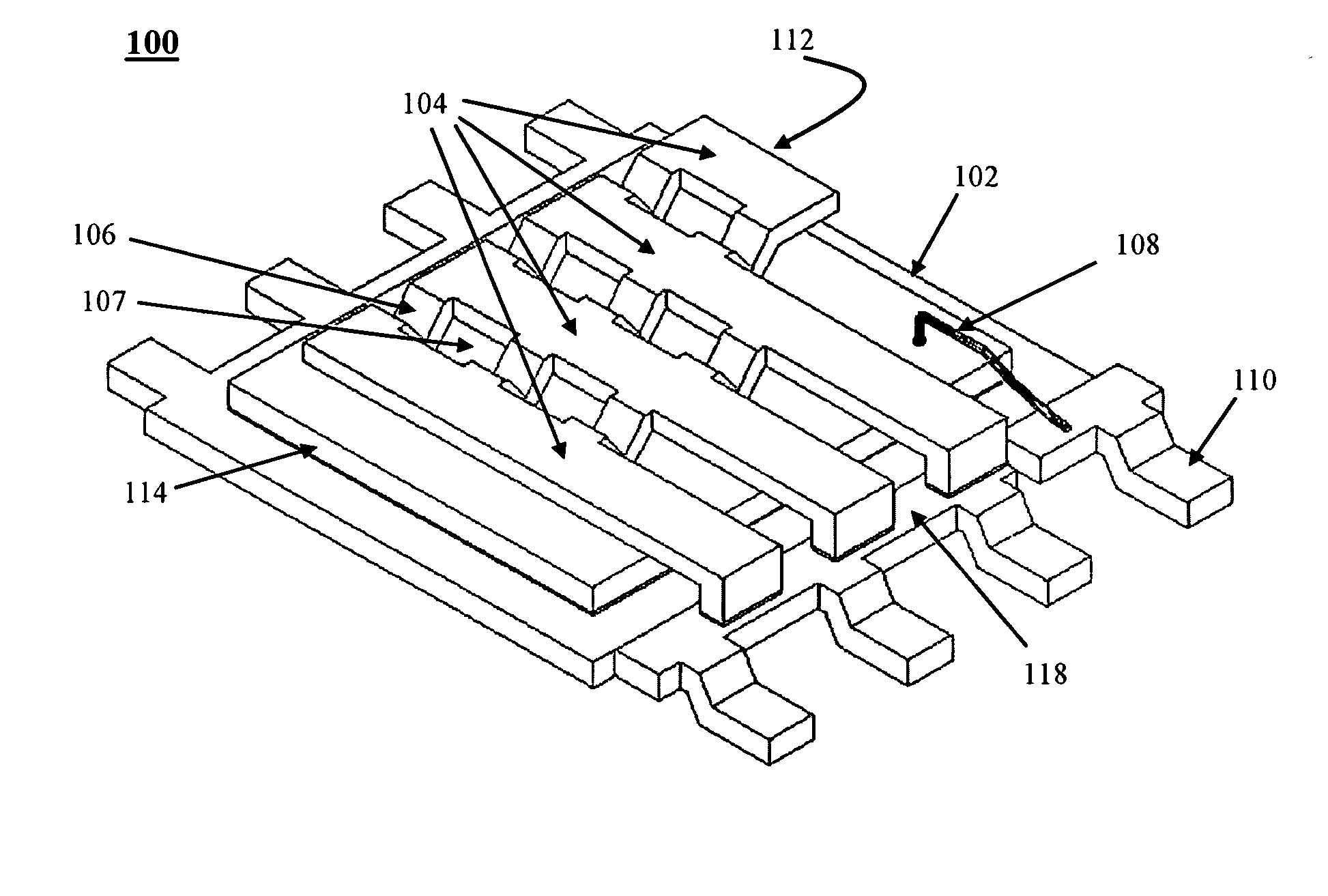
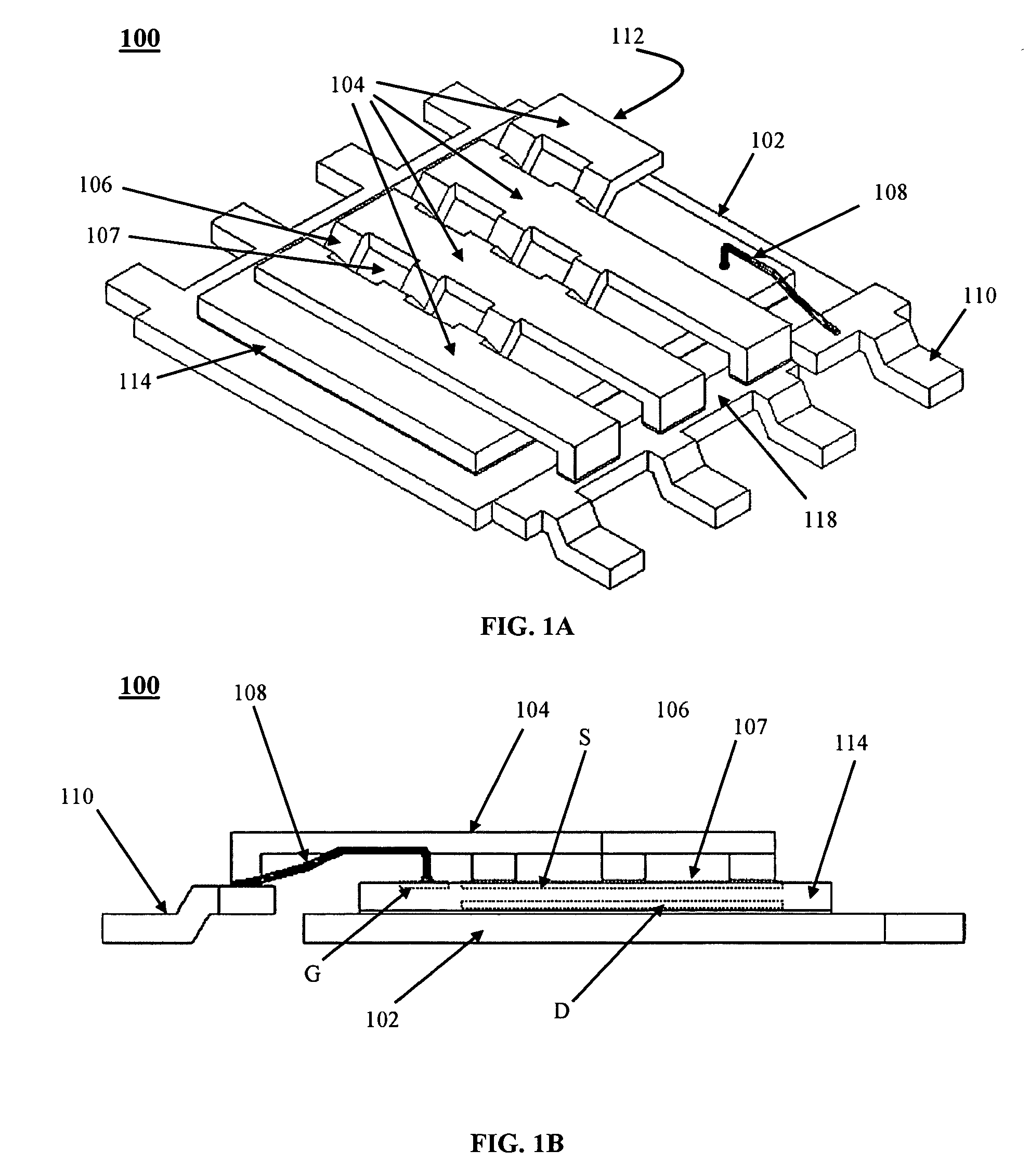
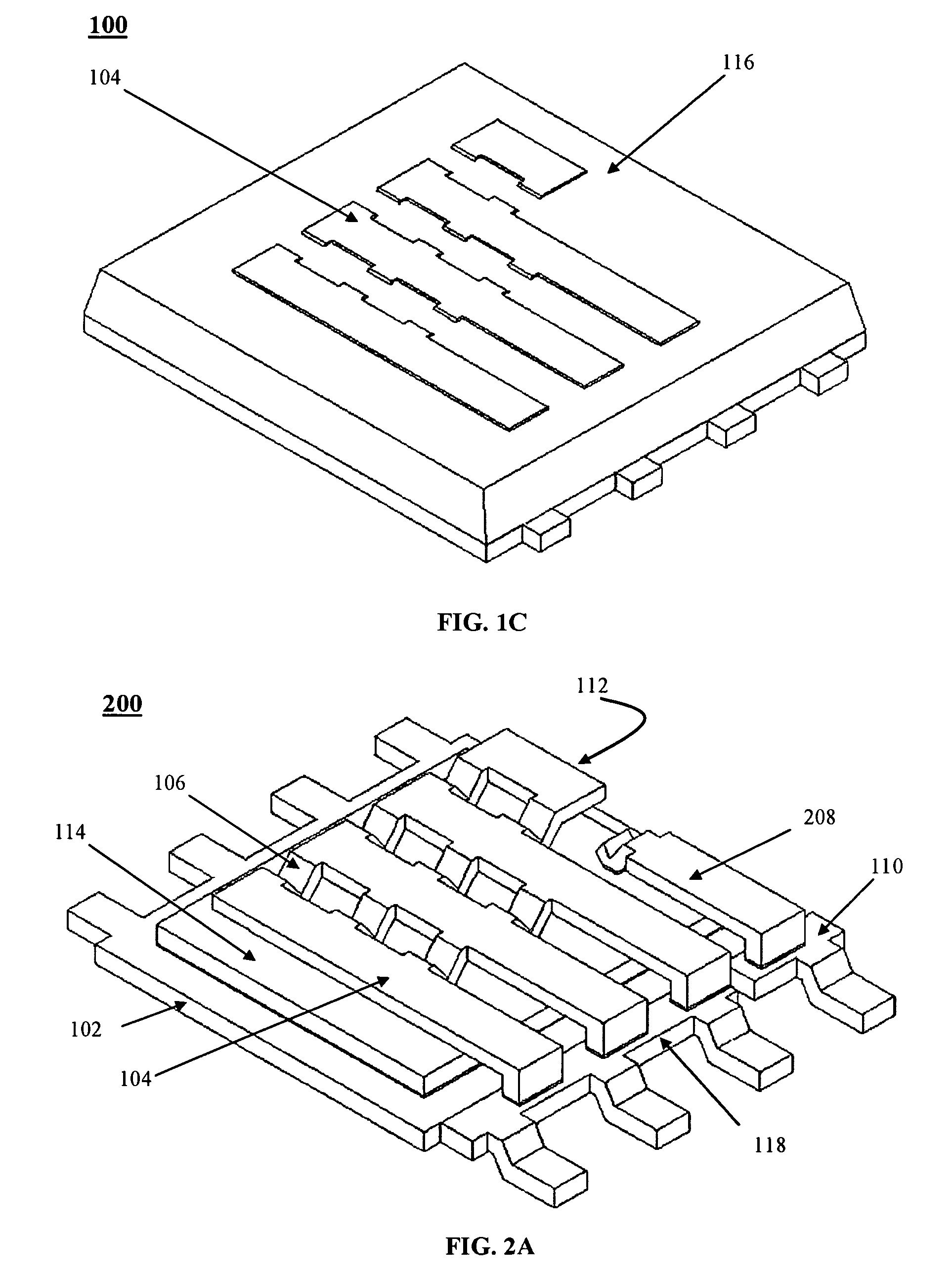
[0031]According to one embodiment of the present invention, as depicted in FIGS. 1A-1B, a semiconductor device package 100 may have a V-shaped clip with a non-exposed gate wire bonded to a lead frame. As shown in FIG. 1A, the device package 100 includes a fused lead frame 102 and a semiconductor device 114, e.g., a MOS device having a top source S, a top gate G and a bottom drain D located on top of the lead frame 102 with the bottom drain D contacting the main portion of the lead frame 102. By way of example, and not by way of limitation, t...


PUM


Abstract

A clip for a semiconductor device package may include two or more separate electrically conductive fingers electrically connected to each other by one or more electrically conductive bridges. A first end of at least finger is adapted for electrical contact with a lead frame. The bridges are adapted to provide electrical connection to a top semiconductor region of a semiconductor device and may also to provide heat dissipation path when a top surface of the fingers is exposed. A semiconductor device package may include the clip along with a semiconductor device and a lead frame. The semiconductor device may have a first and semiconductor regions on top and bottom surfaces respectively. The clip may be electrically connected to the top semiconductor region at the bridges and electrically connected to the lead frame at a first end of at least one of the fingers.

Description

FIELD OF THE INVENTION[0001]This invention generally relates to semiconductor die packages and more particularly to the use of a source clip in a die package to provide electrical contact in a way that lowers spreading resistance and enhances heat dissipation.BACKGROUND OF THE INVENTION[0002]In semiconductor device packaging, a metallic clip is often used to provide electrical connections between a semiconductor die and a lead frame to which the die is mounted. For example, U.S. Pat. No. 6,624,522 discloses a metal oxide semiconductor (MOS) gated device wafer having a source side covered with a passivation layer, preferably a photosensitive liquid epoxy, or a silicon nitride layer, or the like. The wafer is coated by a spinning, screening, or otherwise depositing the liquid epoxy onto the wafer surface. The material is then dried and the coated wafer is exposed using standard photolithographic techniques to image the wafer and openings are formed in the passivation layer to produce ...

Claims


Application Information

Patent Timeline
Patent Type & Authority Patents(United States)
IPC IPC(8): H01L23/495
CPCH01L23/49551H01L24/48H01L2924/13055H01L2924/3025H01L2924/014H01L24/34H01L24/40H01L2924/13091H01L2924/01005H01L2223/54486H01L2924/01033H01L24/83H01L2924/01082H01L2224/73219H01L23/49568H01L2224/48465H01L2224/83801H01L24/28H01L2224/73221H01L24/39H01L24/73H01L24/29H01L23/49524H01L23/4334H01L2924/19041H01L23/544H01L2924/01006H01L23/49562H01L24/41H01L2924/01078H01L2924/19043H01L2924/01023H01L2224/48247H01L2224/32245H01L2224/451H01L2924/1301H01L2924/1305H01L2924/1306H01L2924/00014H01L2924/181H01L2224/40095H01L2224/40245H01L2224/48095H01L2224/37011H01L2224/371H01L24/37H01L2224/83192H01L2224/84815H01L24/84H01L2224/84345H01L2924/00H01L2924/00012H01L2924/3512H01L2224/45099H01L2224/05599
Inventor SHI, LEILIU, KAISUN, MING
Owner ALPHA & OMEGA SEMICON LTD
Why Eureka
Try Eureka