LED package and LED package mounting structure

a technology for led packages and mounting structures, applied in the direction of sustainable manufacturing/processing, instruments, final product manufacturing, etc., can solve the problems of increasing the solder thickness, reducing the mounting accuracy of the led package relative to the circuit board, and generating and propagating cracks in the solder joints. , to achieve the effect of low cos

Inactive Publication Date: 2014-05-06
MAXELL HLDG LTD
View PDF17 Cites 5 Cited by
  • Summary
  • Abstract
  • Description
  • Claims
  • Application Information

AI Technical Summary

Benefits of technology

[0011]In view of the problems mentioned above, an object of the present invention is to provide an LED package and an LED package mounting structure which can improve the fatigue life of solder which electrically connects an LED package and a circuit board even when there is a difference in the coefficients of linear expansion between the LED package and the circuit board, and prevent continuity failure at low costs.
[0016]According to the present invention, even when there is a difference in the coefficients of linear expansion between the LED package and the circuit board, the fatigue life of solder which electrically connects the LED package and the circuit board can be improved, and the LED package and LED package mounting structure which can prevent continuity failure can be provided at low costs.

Problems solved by technology

H7-115227 on a circuit board by soldering entails the problem that the difference in the coefficients of linear expansion between the LED package and the circuit board generates and propagates cracks in the solder joint below the electrodes of the LED package due to changes in temperature caused by turning on / off the LED and finally continuity failure is caused by fatigue fracture of the solder joint.
A possible solution for the problem stated above is increasing the amount of solder provided to increase the solder thickness in the joint portion, but increasing the solder thickness lowers the mounting accuracy of the LED package relative to the circuit board.
That is, an increased positional shift of the LED package in the front-back and left-right directions, or inclination or rotation of the light-emitting surface of the LED package in the front-back direction lowers its optical coupling efficiency with the light guide plate.
Another possible solution is to employ other connection means such as a thermosetting resin containing solder as a substitution for solder, but it is not practical since it leads to increased costs of components.

Method used


Image

  • LED package and LED package mounting structure
  • LED package and LED package mounting structure
  • LED package and LED package mounting structure

Examples


first embodiment

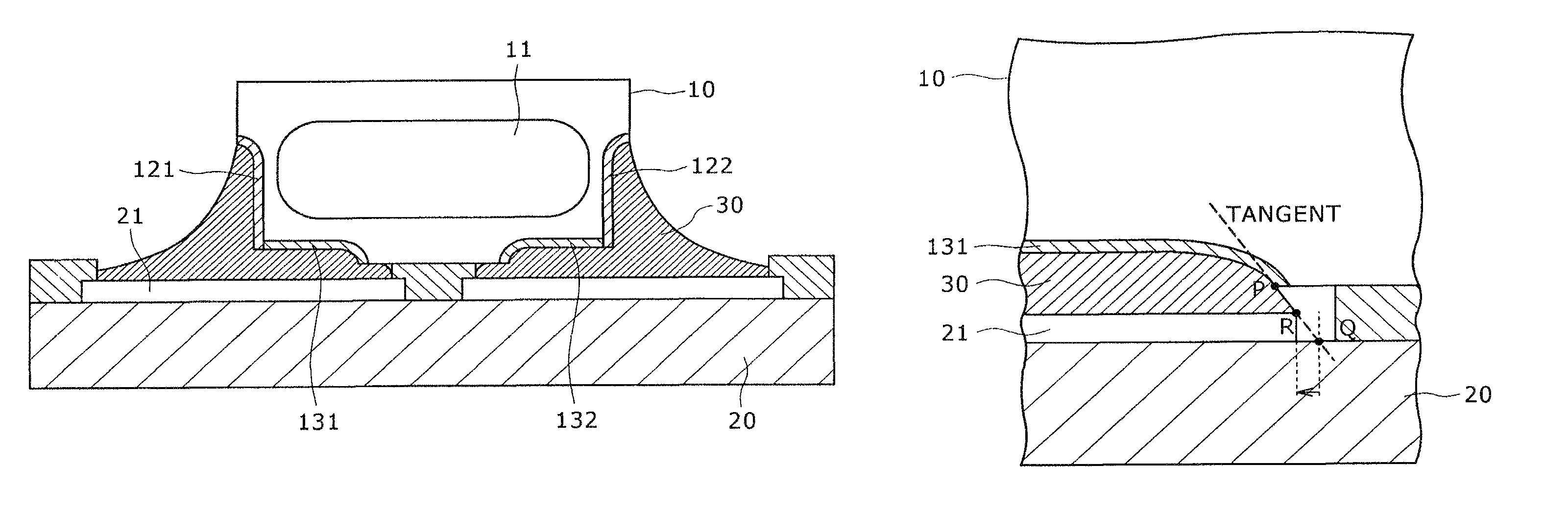
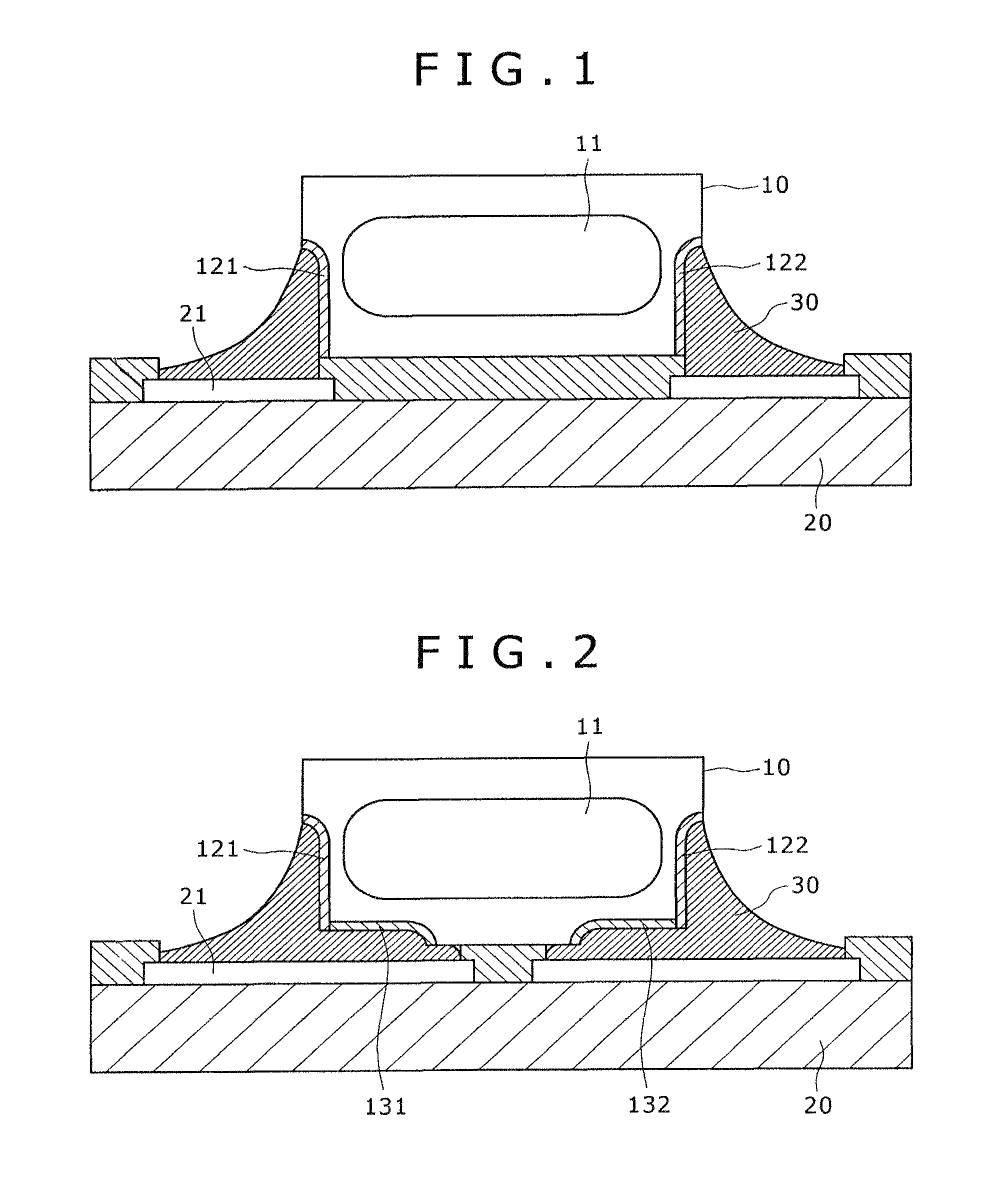
[0026]FIG. 1 shows a schematic front cross-sectional view of an LED package and an LED package mounting structure according to the first embodiment of the present invention.

[0027]The LED package mounting structure comprises a surface mount type LED package 10 which is electrically connected to a circuit board 20 via solder. Herein, the LED package 10 has a case made of a ceramic sintered body produced by laminating a plurality of green sheets comprising alumina as a main component and calcining the same, and an LED element (not shown) is mounted inside the case. As the ceramic material, aluminium nitride, silicon carbide and beryllium oxide may be used, in addition to alumina. A resin package such as polyamide may be used in place of the ceramic package mentioned above.

[0028]The material used for the circuit board on which the LED package is mounted may be relatively inexpensive organic resin substrates such as glass epoxy board, as well as ceramic-based substrates having excellent ...

second embodiment

[0037]FIG. 2 shows a schematic front cross-sectional view of an LED package and an LED package mounting structure according to the second embodiment of the present invention. The embodiment is a partial modification of the first embodiment above, where like portions having similar functions to those in the above-described embodiment are designated by like numerals, and detailed description for like parts are omitted.

[0038]The material of the LED package in the LED package mounting structure according to the second embodiment and the material of the circuit board on which the LED package is mounted are the same as those in the LED package mounting structure of the first embodiment. However, the LED package mounting structure according to the second embodiment has a structural difference from that according to the first embodiment. The LED package mounting structure according to the second embodiment is characterized in that it has connection terminal portions not only on the side fac...

third embodiment

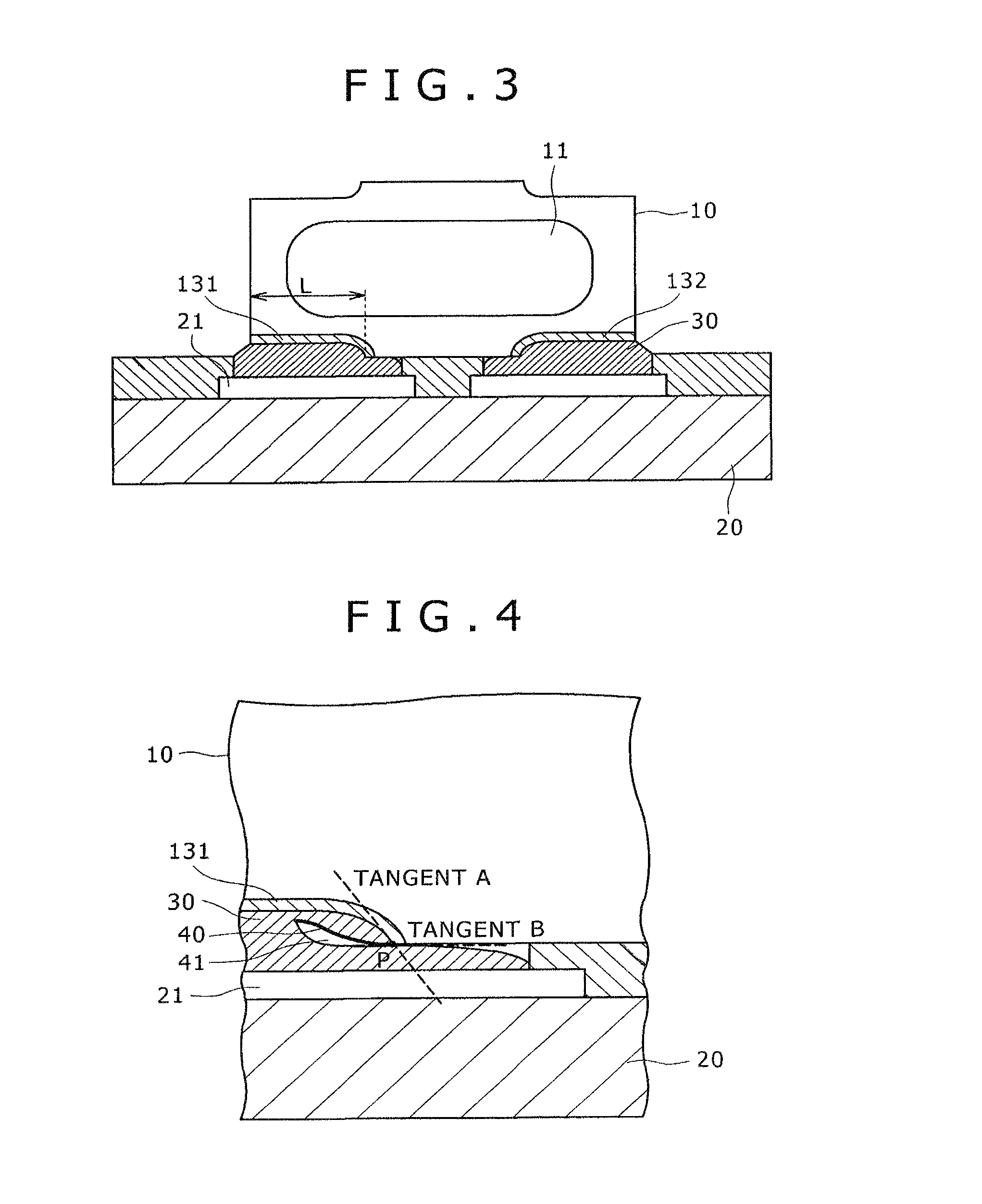
[0047]FIG. 5 shows an enlarged cross-sectional view of the electrode portion on the bottom face of the package in the LED package and LED package mounting structure according to the third embodiment of the present invention. In the LED package mounting structure according to the third embodiment, as in the LED package mounting structure according to the second embodiment of the present invention shown in FIG. 2, connection terminal portions may be provided on the bottom face and side face, respectively, of the LED package, or as in the LED package mounting structure according to Comparative Example 1 shown in FIG. 3, the connection terminal portions may be provided only on the bottom face of the LED package. In either case, the LED package and LED package mounting structure according to the third embodiment of the present invention comprise the connection terminal portions for connecting with the circuit board on at least the bottom face of the LED package, and are mounted on the ci...


PUM


Abstract

A highly reliable LED package mounting structure which can realize improvement in solder fatigue life at low costs is provided. An LED package has a light-emitting surface which is perpendicular to a mounting surface of a circuit board, comprises connection terminal portions on the side face or on the side face and the bottom face of the package, and is joined with the circuit board by soldering via the connection terminal portion. Furthermore, the shape of the solder is optimized by defining the relative position relation between the end of an electrode on the central side of the LED package on the bottom face of an LED package body and the end of a component mounting pad on the circuit board.

Description

CROSS-REFERENCES TO RELATED APPLICATIONS[0001]This application relates to and claims priority from Japanese Patent Application No. 2010-080104, filed on Mar. 31, 2010, the entire disclosure of which is incorporated herein by reference.BACKGROUND OF THE INVENTION[0002]1. Field of the Invention[0003]The present invention relates to an LED package, an LED package mounting structure comprising an LED package mounted on a circuit board such as a printed circuit board, and a liquid crystal display comprising an LED package mounting structure.[0004]2. Description of the Related Art[0005]In recent years, LEDs are increasingly used as light sources of backlight units for liquid crystal displays of televisions and monitors. This current corresponds to the demands for improved efficiencies of liquid crystal displays, and by using LED light sources, the power consumption and thickness of television sets can be reduced than in conventional cold cathode fluorescent tubes. In particular, by realiz...

Claims


Application Information

Patent Timeline
Patent Type & Authority Patents(United States)
IPC IPC(8): H01L23/52
CPCH05K3/3442H01L33/62H01L2224/16H01L33/486H05K2201/09472H05K2201/10106Y02P70/50
Inventor KASHIMURA, TAKASHIYAMAZAKI, TETSUYA
Owner MAXELL HLDG LTD
Why Eureka
Try Eureka