Method for producing semiconductor device and semiconductor device

a technology of semiconductor devices and semiconductors, applied in the direction of semiconductor devices, electrical equipment, transistors, etc., can solve the problem of hard to reduce the area occupied by the circuit, and achieve the effect of reducing the parasitic capacitance between the gate line and the substrate, reducing the parasitic capacitance, and easy production

Active Publication Date: 2014-05-27
UNISANTIS ELECTRONICS SINGAPORE PTE LTD
View PDF12 Cites 29 Cited by
  • Summary
  • Abstract
  • Description
  • Claims
  • Application Information

AI Technical Summary

Benefits of technology

[0019]The present invention can provide a SGT production method in which the parasitic capacitance between a gate line and a substrate is decreased, a gate last process is employed, and two transistors are produced from a single dummy pattern and a SGT structure formed by the production method.
[0020]Two SGTs can be easily produced from a single dummy pattern by employing a method for producing an existing FINFET. In the method, a sidewall is formed around a dummy pattern and a substrate is etched using the sidewall as a mask to form a fin, and thus two transistors are formed from a single dummy pattern.
[0021]In addition, a metal gate SGT can be easily produced because a production method that employs an existing metal gate last process can be used. A silicide has been conventionally formed in an upper portion of a pillar-shaped silicon layer, but the temperature at which a polysilicon is deposited is higher than the temperature at which a silicide is formed and thus a silicide needs to be formed after the formation of a polysilicon gate. If a silicide is formed in an upper portion of a silicon pillar, a polysilicon gate is formed, a hole is made above a polysilicon gate electrode, an insulating film is formed on the sidewall of the hole, a silicide is formed, and the hole is filled with an insulating film. This increases the number of production steps. Therefore, the existing metal gate last process below can be employed. A diffusion layer is formed before the formation of a polysilicon gate electrode and a polysilicon gate line. By covering a pillar-shaped silicon layer with the polysilicon gate electrode and by forming a silicide only in an upper portion of a fin-shaped silicon layer, a polysilicon gate is formed. Subsequently, an interlayer insulating film is deposited and then the polysilicon gate is exposed by chemical mechanical polishing. The polysilicon gate is etched and then a metal is deposited.

Problems solved by technology

Such a decrease in the size of MOS transistors causes difficulty in suppressing leak currents, which poses a problem in that it is hard to reduce the area occupied by the circuits because of the requirements of the secure retention of necessary currents.
However, the production process after a metal gate is formed needs to be conducted always in consideration of metal contamination due to the metal gate.

Method used


Image

  • Method for producing semiconductor device and semiconductor device
  • Method for producing semiconductor device and semiconductor device
  • Method for producing semiconductor device and semiconductor device

Examples


Embodiment Construction

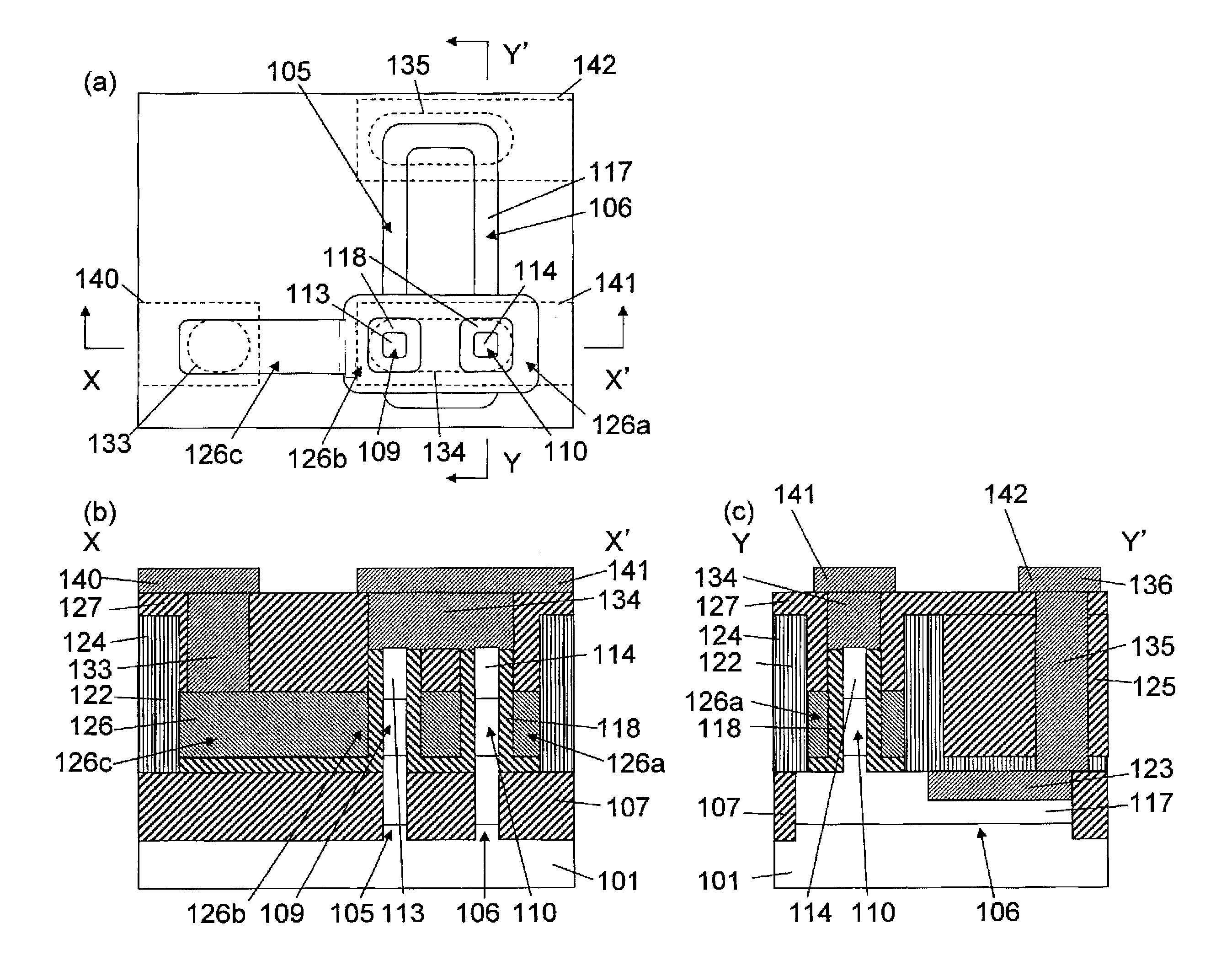
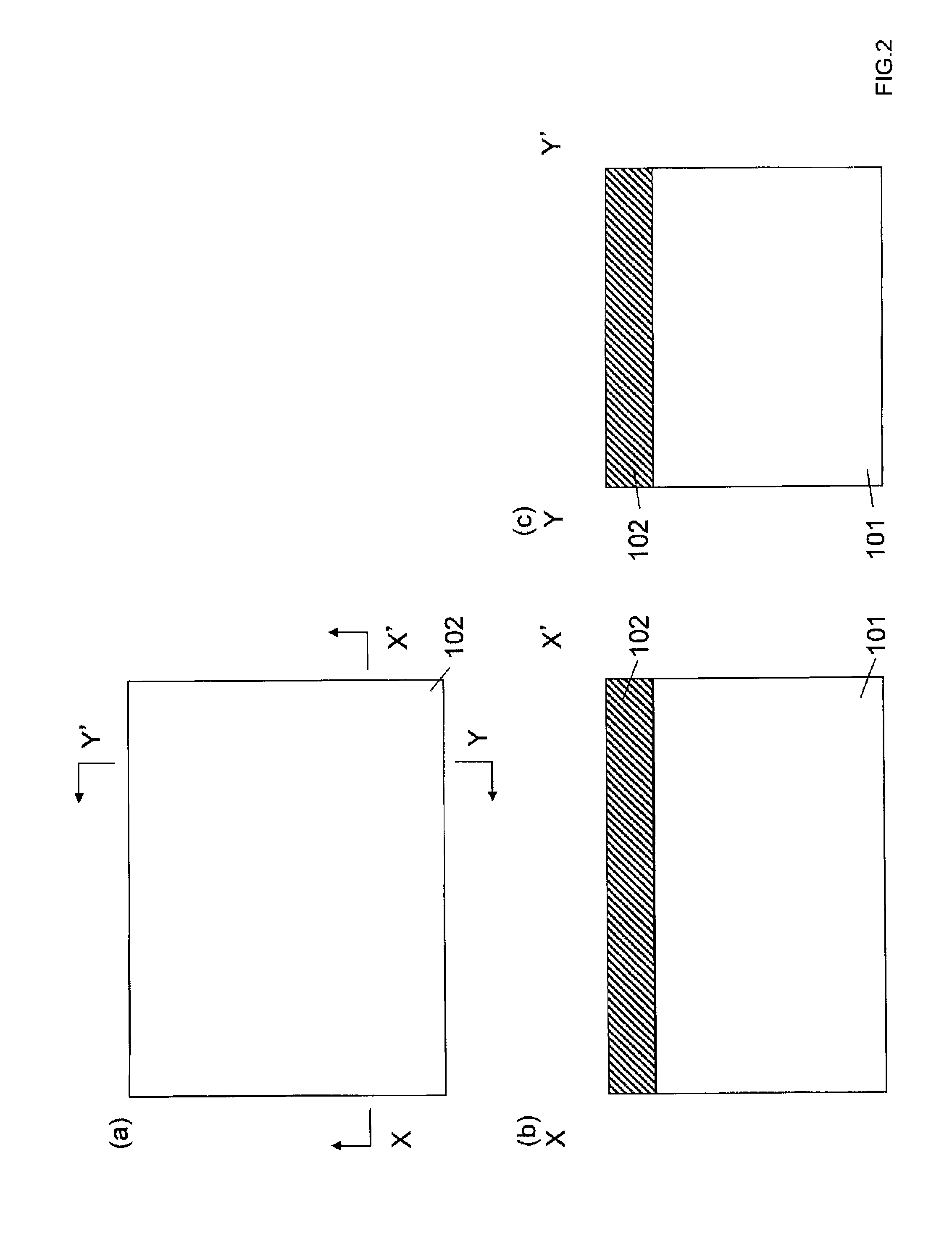
[0069]A production process for forming a SGT structure according to an embodiment of the present invention will now be described with reference to FIGS. 2 to 47.

[0070]A production method is described that includes forming a first fin-shaped silicon layer and a second fin-shaped silicon layer on a substrate, forming a first insulating film around the first fin-shaped silicon layer and second fin-shaped silicon layer, forming a first pillar-shaped silicon layer in an upper portion of the first fin-shaped silicon layer, and forming a second pillar-shaped silicon layer in an upper portion of the second fin-shaped silicon layer. As shown in FIG. 2, a second oxide film 102 is deposited on a silicon substrate 101 in order to form a dummy pattern. A nitride film or a laminated film of an oxide film and a polysilicon may be used.

[0071]As shown in FIG. 3, a first resist 103 for forming the dummy pattern is formed.

[0072]As shown in FIG. 4, the second oxide film 102 is etched to form the dummy ...


PUM

PropertyMeasurementUnit
temperatureaaaaaaaaaa
widthaaaaaaaaaa
sizeaaaaaaaaaa

Abstract

A SGT production method includes a step of forming first and second fin-shaped silicon layers, forming a first insulating film, and forming first and second pillar-shaped silicon layers; a step of forming diffusion layers by implanting an impurity into upper portions of the first and second pillar-shaped silicon layers, upper portions of the first and second fin-shaped silicon layers, and lower portions of the first and second pillar-shaped silicon layers; a step of forming a gate insulating film and first and second polysilicon gate electrodes; a step of forming a silicide in upper portions of the diffusion layers formed in the upper portions of the first and second fin-shaped silicon layers; and a step of depositing an interlayer insulating film, exposing and etching the first and second polysilicon gate electrodes, then depositing a metal, and forming first and second metal gate electrodes.

Description

RELATED APPLICATIONS[0001]Pursuant to 35 U.S.C. §119(e), this application claims the benefit of the filing date of Provisional U.S. Patent Application Ser. No. 61 / 566,244 filed on Dec. 2, 2011. The entire content of this application is hereby incorporated by reference.BACKGROUND OF THE INVENTION[0002]1. Field of the Invention[0003]The present invention relates to a semiconductor device.[0004]2. Description of the Related Art[0005]The degree of integration of semiconductor integrated circuits, in particular, integrated circuits using MOS transistors, has been increasing. With the increasing degree of integration, the size of MOS transistors used in integrated circuits has been decreased to nano-scale dimensions. Such a decrease in the size of MOS transistors causes difficulty in suppressing leak currents, which poses a problem in that it is hard to reduce the area occupied by the circuits because of the requirements of the secure retention of necessary currents. To address the proble...

Claims


Application Information

Patent Timeline
Patent Type & Authority Patents(United States)
IPC IPC(8): H01L29/78H01L29/66H01L21/336
CPCH01L29/7827H01L29/456H01L29/0657H01L29/66666H01L29/495H01L21/823437H01L21/02532H01L21/823487H01L21/823475H01L29/66545H01L21/32133H01L29/42392H01L29/66742H01L29/78618H01L29/78642H01L29/78696
Inventor MASUOKA, FUJIONAKAMURA, HIROKI
Owner UNISANTIS ELECTRONICS SINGAPORE PTE LTD
Why Eureka
Try Eureka