Quad flat non-leaded package structure with electromagnetic interference shielding function and method for fabricating the same

a non-leaded, electromagnetic interference shielding technology, applied in the direction of electrical equipment, semiconductor devices, semiconductor/solid-state device details, etc., can solve the problems of increasing assembly difficulty, complicated structure fabrication process, adversely affecting electrical performance of the overall package structure, etc., to overcome the conventional drawback of turbulence, facilitate mass production, and improve the effect of electrical connection quality

Active Publication Date: 2014-05-27
SILICONWARE PRECISION IND CO LTD
View PDF19 Cites 9 Cited by
  • Summary
  • Abstract
  • Description
  • Claims
  • Application Information

AI Technical Summary

Benefits of technology

[0017]According to the present invention, the grooves are formed in the encapuslant before a singulation process so as to allow the EMI shielding film to be formed therein and in contact with the connection strips, thus achieving an EMI shielding function and facilitating mass production.
[0018]Further, the present invention overcomes the conventional drawback of turbulence which occurs when the encapsulant passes through a perforated metal shield, thus avoiding generation of air bubbles in the encapsulant and the popcorn effect caused thereby. Furthermore, since the shielding film and the supporting portions are in surface contact, it ensures higher electrical connection quality compared with the point contact of the prior art.

Problems solved by technology

However, such a package size can easily be influenced by external EMI noises during operation, thus adversely affecting electrical performance of the overall package structure.
However, since an additionally fabricated metal shield 13 is required in the above-described structure, the fabrication process of the structure is complicated.
Further, the metal shield 13 is required to cover the chip 11 and fixed to the substrate 10, thus increasing the assembly difficulty.
However, since the metal layer 24 must be formed after a singulation process and it is difficult to perform component arrangement and pickup in a singulated package structure, the above structures are not suitable for mass production.
In addition, the sputtering process cannot be applied in a package structure in which the encapsulant is flush with the substrate.
However, the conductive wire layer is made of a non-ferrous metal material and can only be formed on the groove and encapsulant by depositing or sputtering.
Therefore, it cannot be applied in a package structure in which the encapsulant is flush with the substrate.
Further, the contact between the conductive wire layer and the bonding wires is point contact, which can easily result in poor electrical connection between the conductive wire layer and the bonding wires.

Method used


Image

  • Quad flat non-leaded package structure with electromagnetic interference shielding function and method for fabricating the same
  • Quad flat non-leaded package structure with electromagnetic interference shielding function and method for fabricating the same
  • Quad flat non-leaded package structure with electromagnetic interference shielding function and method for fabricating the same

Examples


Embodiment Construction

[0025]The following illustrative embodiments are provided to illustrate the disclosure of the present invention, these and other advantages and effects can be apparent to those in the art after reading this specification.

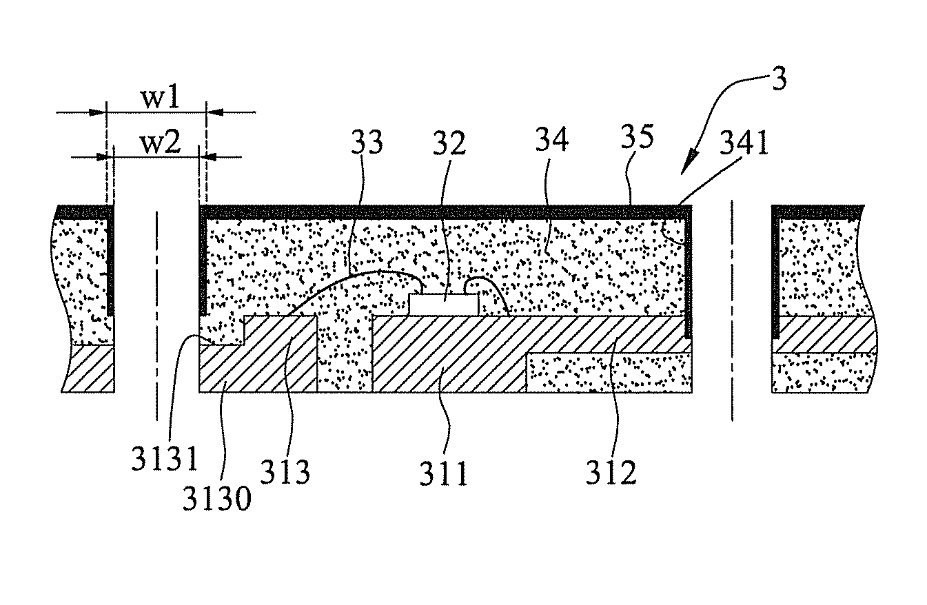
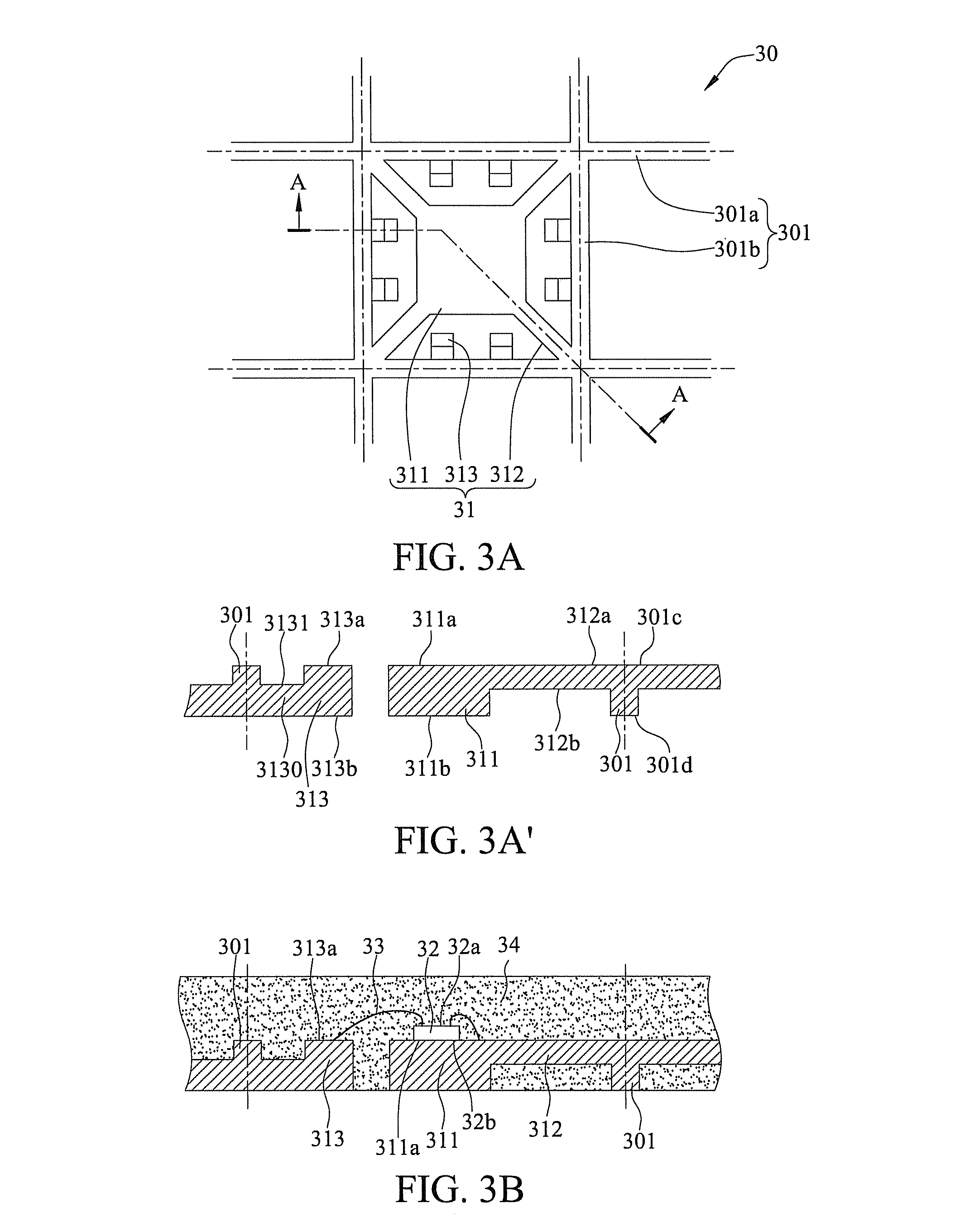
[0026]Please refer to FIGS. 3A, 3A′, 3B, 3C, 3D, and 3E for the drawings of a fabrication method of a QFN package structure with an EMI shielding function according to the present invention. FIG. 3A is a top view. FIG. 3A′ is a cross-sectional view taken along a line A-A in FIG. 3A. FIGS. 3B, 3C, 3D, and 3E are cross-sectional views.

[0027]Referring to FIGS. 3A and 3A′, a metal frame 30 made of copper is provided, which comprises a plurality of lead frames 31 and a plurality of connection strips 301 composed of a plurality of transverse connection strips 301a and a plurality of longitudinal connection strips 301b. Each of the lead frames 31 has a die pad 311, a plurality of supporting portions 312 connecting to the die pad 311, and a plurality of leads 313 disposed a...


PUM


Abstract

A quad flat non-leaded (QFN) package structure with an electromagnetic interference (EMI) shielding function is proposed, including: a lead frame having a die pad, a plurality of supporting portions connecting to the die pad and a plurality of leads disposed around the periphery of the die pad without connecting to the die pad; a chip mounted on the die pad; bonding wires electrically connecting the chip and the leads; an encapsulant for encapsulating the chip, the bonding wires and the lead frame and exposing the side and bottom surfaces of the leads and the bottom surface of the die pad; and a shielding film disposed on the top and side surfaces of the encapsulant and electrically connecting to the supporting portions for shielding from EMI. A method of fabricating the package structure as described above is further proposed.

Description

CROSS-REFERENCES TO RELATED APPLICATIONS[0001]This application claims under 35 U.S.C. §119(a) the benefit of Taiwanese Application No. 099104606 filed Feb. 12, 2010 the entire contents of which is incorporated herein by reference.BACKGROUND OF THE INVENTION[0002]1. Field of the Invention[0003]The present invention relates to package structures and methods for fabricating the same, and more particularly, to a quad flat non-leaded (QFN) package structure with an electromagnetic interference (EMI) shielding function and a method for fabricating the same.[0004]2. Description of Related Art[0005]Generally, a lead frame can be used as a chip carrier, which has a die pad and a plurality of leads formed around the periphery of the base. A chip can be mounted to the die pad and electrically connected to the leads through bonding wires. Further, an encapsulant can be formed to encapsulate the chip, the die pad, the bonding wires and the inner portions of the leads so as to form a semiconducto...

Claims


Application Information

Patent Timeline
Patent Type & Authority Patents(United States)
IPC IPC(8): H01L23/552
CPCH01L2224/49H01L2924/01006H01L23/49548H01L24/97H01L24/48H01L2924/01082H01L23/3107H01L21/561H01L24/49H01L23/552H01L2224/48247H01L2924/3025H01L2924/01029H01L2224/48091H01L2224/97H01L24/96H01L2224/48257H01L2924/01033H01L2924/00014H01L2924/181H01L2224/85H01L2224/45099H01L2224/05599H01L2924/00012
Inventor YAO, CHIN-TSAIHUANG, CHIEN-PINGKE, CHUN-CHI
Owner SILICONWARE PRECISION IND CO LTD
Why Eureka
Try Eureka