Metal foil with electric resistance film and method of producing the same

a metal foil and electric resistance technology, applied in the direction of resistor details, printed resistor incorporation, transportation and packaging, etc., can solve the problems of reducing the conventional technology stops at forming, etc., and achieves significant simplified mounting process, reduced space, and reduced the effect of the number of parts to be mounted or soldered

Active Publication Date: 2014-06-10
JX NIPPON MINING & METALS CORP
View PDF12 Cites 2 Cited by
  • Summary
  • Abstract
  • Description
  • Claims
  • Application Information

AI Technical Summary

Benefits of technology

[0009]With conventionally used built-in resistor elements, one resistor element is configured of one type of substance on the copper foil. Nevertheless, when actually mounting the resistor elements, the circuit design tolerance can be increased and the number of man-hours can be reduced with two resistor elements and further with a plurality of resistor elements compared to a case with one resistor element. Thus, an object of this invention is to provide a metal foil with a built-in resistor element comprising two or more types of resistor elements on one metal foil.
[0010]As a result of intense study to overcome the foregoing problems, the present inventors, etc. discovered that a metal foil with a built-in resistor element having two or more types of resistor elements on one metal foil is effective and can be produced relatively easily.
[0018]As a result of using the copper foil with two or more types of built-in electric resistance film layers of the present invention, it is no longer necessary to independently form a separate electric resistance element upon designing the circuit, and, since it is only necessary to expose the resistive element of the electric resistance film layer formed on the copper foil using an etching solution such as copper chloride, solder bonding becomes unneeded or is considerably alleviated, and an effect is yielded in that the mounting process is significantly simplified.
[0019]Moreover, as a result of the number of parts to be mounted or soldered being reduced, there is also an advantage in that the space can be expanded and downsizing / weight-saving can be achieved. It is thereby possible to improve the freedom of circuit design. In addition, as a result of two or more types of resistor elements being built into the copper foil, an additional effect is yielded in that signal properties are improved in the high frequency region.

Problems solved by technology

Nevertheless, conventional technology stopped at forming a specific electric resistance film on the metal foil, and there was no concept of forming various types of electric resistance films on the metal foil.[Patent Document 1] Japanese Patent No. 3311338[Patent Document 2] Japanese Patent No. 3452557

Method used


Image

  • Metal foil with electric resistance film and method of producing the same
  • Metal foil with electric resistance film and method of producing the same
  • Metal foil with electric resistance film and method of producing the same

Examples


Embodiment Construction

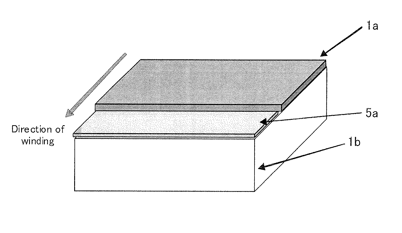
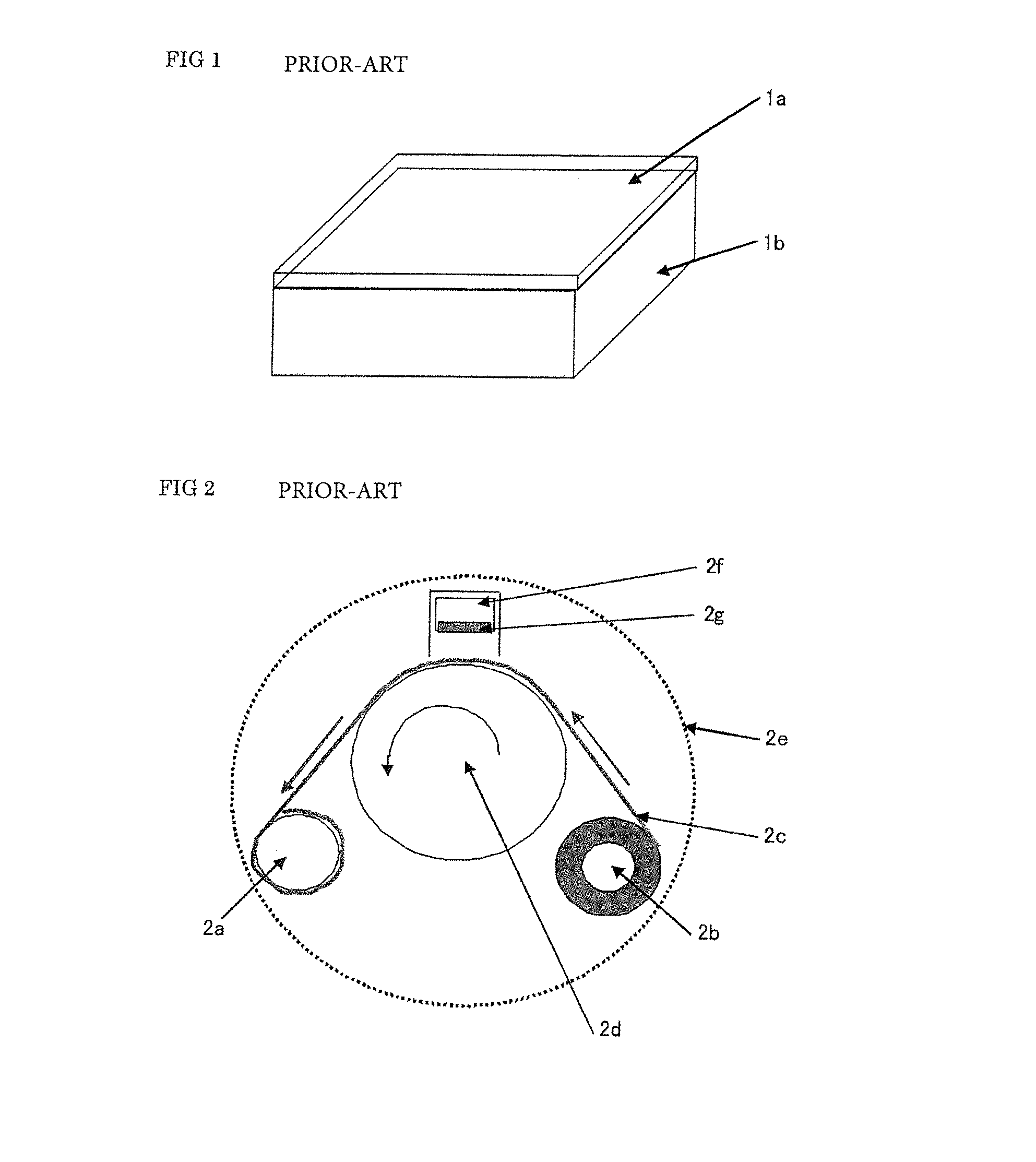
[0030]The structure of a conventional copper foil with a built-in resistor element is shown in FIG. 1. Reference numeral 1a is the built-in thin film resistor element, and reference numeral 1b is the base copper foil. The thin film resistor element 1a is made of NiCr or the like, and is formed based on a manufacturing method of performing sputtering to the surface of the copper foil while winding the copper foil.

[0031]FIG. 2 and FIG. 3 are explanatory diagrams showing the production example of a conventional copper foil with a built-in resistor element. In FIG. 2, the copper foil 2c wound around a rewind roller 2b is wound with a winding roller 2a via a rotating cooling drum 2d.

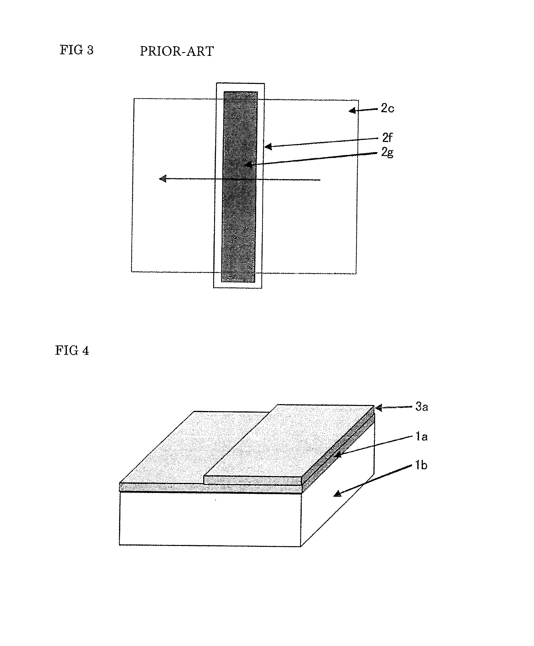
[0032]Argon gas is introduced into a vacuum chamber 2e and the pressure is retained at approximately 0.4 pa. Subsequently, when high voltage is applied to a cathode 2f, a plasma state is realized and the target material 2g is discharged and sputtered on the copper foil.

[0033]FIG. 3 is a plan view showing the...


PUM

PropertyMeasurementUnit
thicknessaaaaaaaaaa
thicknessaaaaaaaaaa
thicknessaaaaaaaaaa

Abstract

A copper foil with an electric resistance film in which a film with higher electrical resistivity than the metal foil is provided on the metal foil, wherein a plurality of electric resistance films with different electric resistance is arranged in parallel on the same metal foil. With conventionally used built-in resistor elements, one resistor element is configured of one type of substance on the copper foil. Nevertheless, when actually mounting the resistor elements, the circuit design tolerance can be increased and the number of man-hours can be reduced with two resistor elements and further with a plurality of resistor elements compared to a case with one resistor element. This invention aims to provide a metal foil with a built-in resistor element comprising two or more types of resistor elements on one metal foil.

Description

BACKGROUND OF THE INVENTION[0001]Many electronic devices are configured as a hybrid of parts with different functions. In recent years, there are demands for downsizing and weight-saving these electronic devices from the perspective of mountability, and the efficient arrangement of the respective parts corresponding to the miniaturization of the substrate area or the enlargement of the active device are being demanded. Recently, thin film resistor elements, in particular, are used upon mounting these parts. The present invention relates to a metal foil with an electric resistance film in which a film with electric resistance is formed on a metal foil.[0002]A copper foil is generally used as the wiring material of a printed circuit board. A copper foil is classified into an electrolytic copper foil and a rolled copper foil based on the production method thereof. The thickness of the copper foil can be arbitrarily adjusted from an extremely thin copper foil with a thickness of 5 μm to...

Claims


Application Information

Patent Timeline
Patent Type & Authority Patents(United States)
IPC IPC(8): H01C1/012
CPCH05K2201/0391C23C14/562C23C14/165C23C14/044C23C14/04H05K2201/0355C23C14/542H05K2203/0361H05K1/167C23C14/08Y10T428/12493
Inventor OHSAKA, SHIGEOKUROSAWA, TOSHIONATSUME, TAKASHI
Owner JX NIPPON MINING & METALS CORP
Why Eureka
Try Eureka