Methods for vacuum assisted underfilling

a vacuum assisted and underfilling technology, applied in the direction of auxillary welding devices, soldering apparatus, semiconductor/solid-state device details, etc., can solve the problems of reducing the opportunity for air to be trapped under the underfill, placing obstructions between the edge of the electronic device and the underfill, etc., to reduce the opportunity for air, reduce the amount of air trapped under the electronic device during the underfill operation, and reduce the chance of air

Inactive Publication Date: 2014-08-05
NORDSON CORP
View PDF46 Cites 5 Cited by
  • Summary
  • Abstract
  • Description
  • Claims
  • Application Information

AI Technical Summary

Benefits of technology

[0008]Other embodiments of the invention are directed to methods of blocking air that has been trapped under the underfill from flowing under the electronic device. In one such method, an obstacle is placed between the edge of the electronic device and the underfill prior to applying the vacuum. After applying the vacuum condition, the underfill is heated to a temperature above room temperature to cause flow of the underfill over the obstacle and from at least one exterior edge into the open portion of the space. Forcing the underfill to flow over an obstacle, helps block the air trapped under the underfill from flowing under the electronic device and allows the trapped air to vent prior to reaching the gap under the electrical device
[0009]Yet another embodiment of the invention is directed to a method of exposing a surface of the substrate to a plasma so as to change the wettability of the substrate prior to providing the underfill onto the substrate proximate to at least one exterior edge of the electronic device. This plasma treatment reduces the opportunity for air to be trapped under the underfill. The method further includes evacuating the space to provide a vacuum condition, in the open portion of the space. After evacuating the space to a vacuum condition, the underfill is heated to cause flow of the underfill toward at least one exterior edge and into the open portion of the space. Since the plasma treatment of the substrate reduces the entrapment of air under the underfill, an amount of air trapped under the electronic device during the underfill operation may also be reduced.
[0010]Similar to the plasma treatment method, a glass-like film may be deposited on the substrate so as to provide a more perfectly smooth and flat surface. This flat surface has fewer depressions or imperfections in which air can be trapped when the underfill is positioned on top of the glass-like film. As entrapment of air under the underfill is reduced, an amount of air trapped under the electronic device during the underfill operation may also be reduced.

Problems solved by technology

In one such method, an obstacle is placed between the edge of the electronic device and the underfill prior to applying the vacuum.
This plasma treatment reduces the opportunity for air to be trapped under the underfill.

Method used


Image

  • Methods for vacuum assisted underfilling
  • Methods for vacuum assisted underfilling
  • Methods for vacuum assisted underfilling

Examples


Embodiment Construction

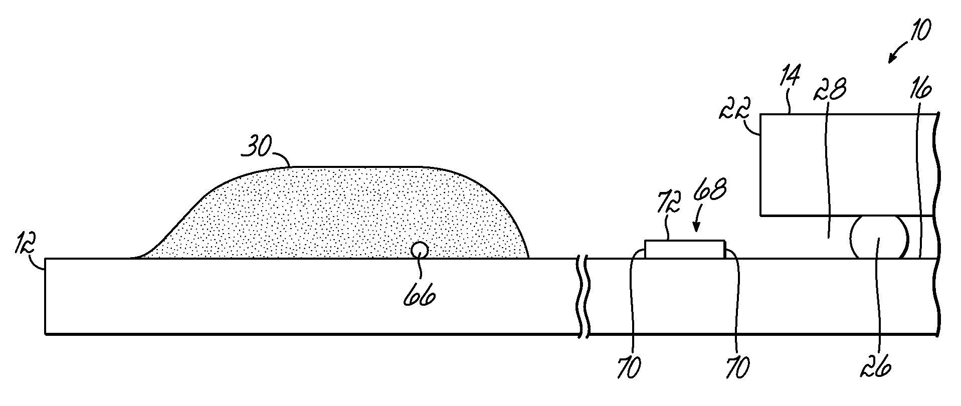
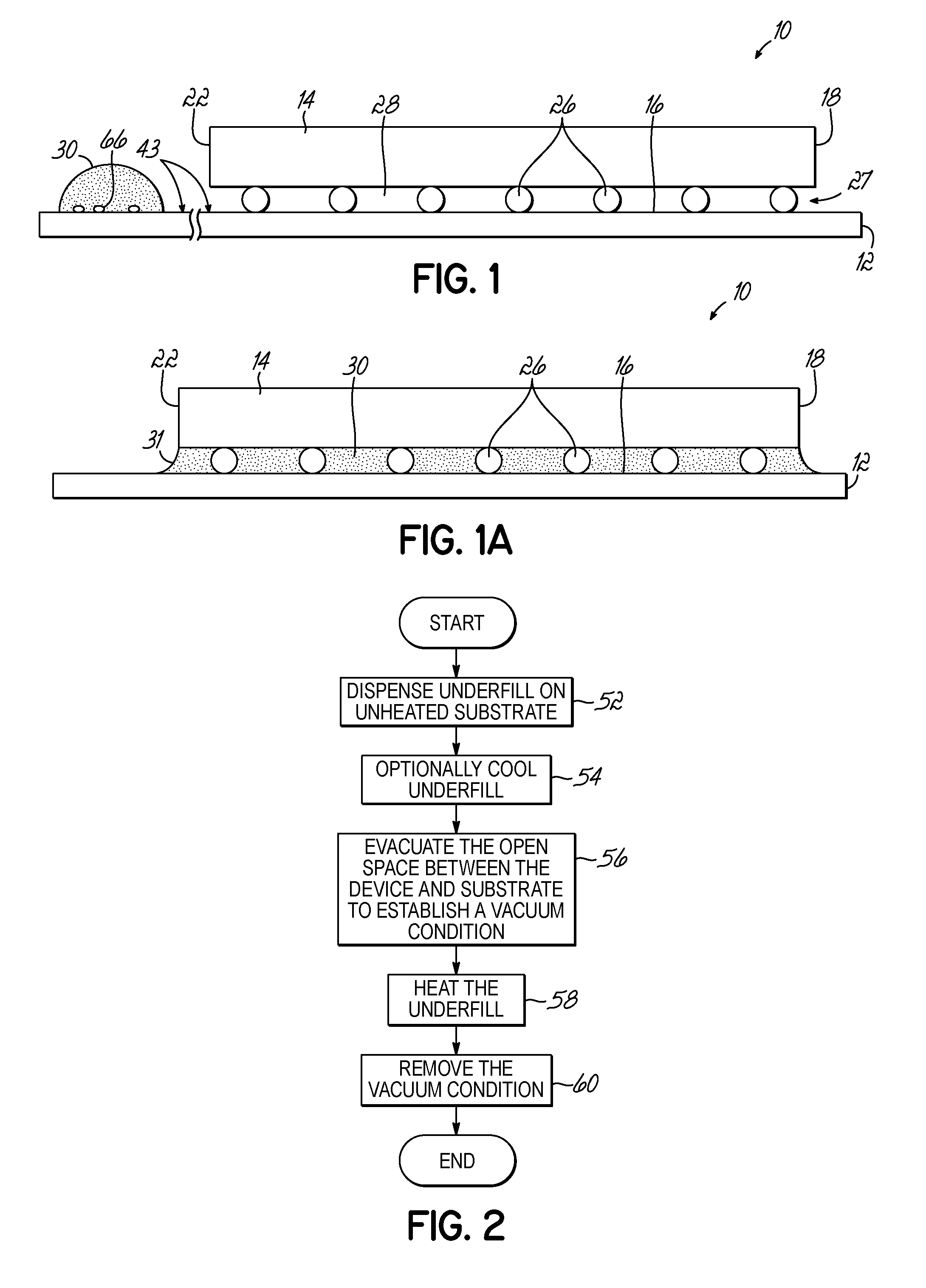
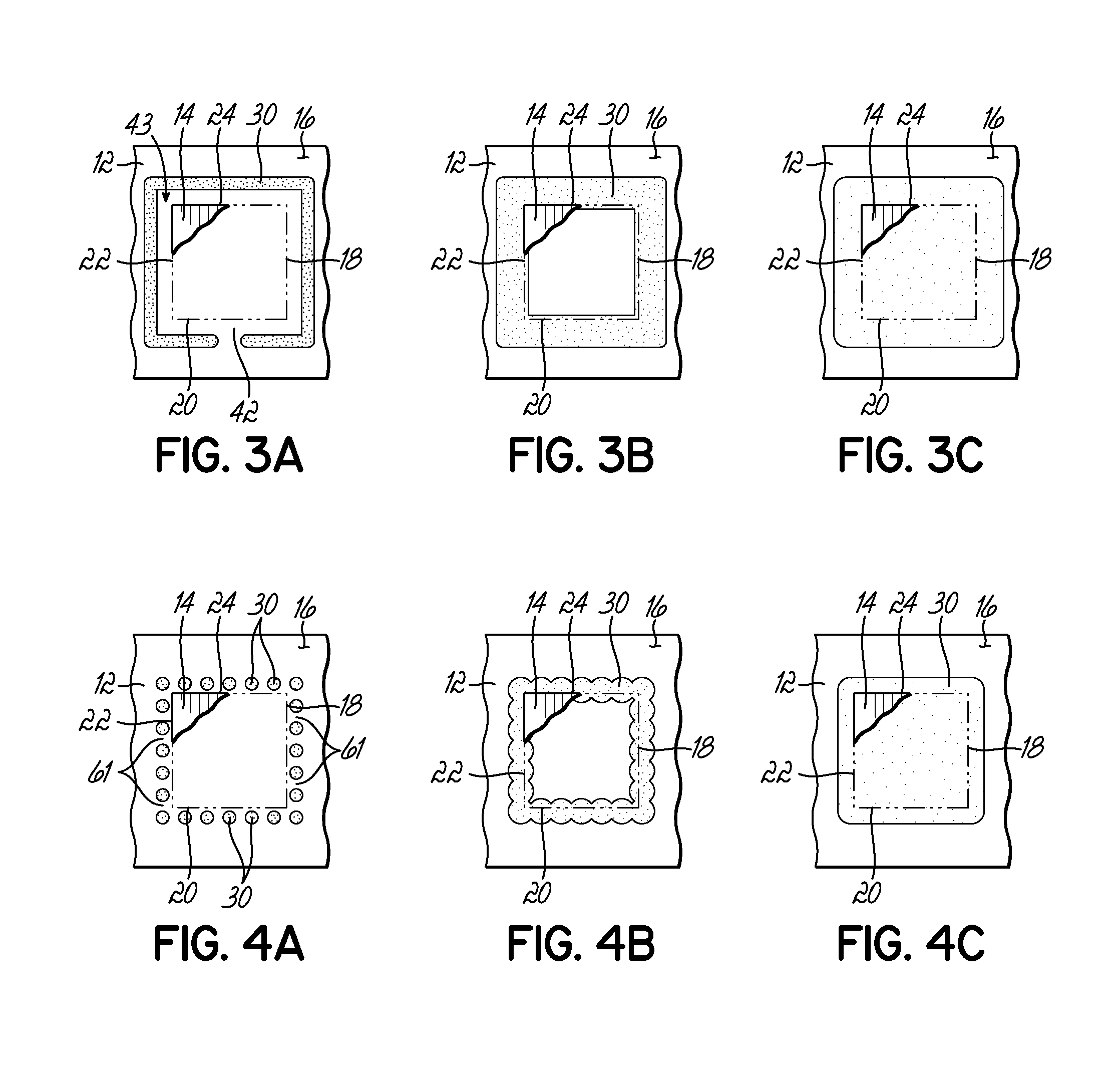
[0029]Generally, the embodiments of the invention are directed to a vacuum-assisted process for underfilling an electronic device mounted on a substrate by an array of solder balls. Underfill is dispensed or otherwise provided (e.g., in either a liquid or solid form) in one or more lines around the edges of an unheated electronic device, which is mounted to an unheated substrate by means of an array of reflowed solder balls. Preferably, at least one gap is left in the one or more lines of underfill and, preferably, if the space between the electronic device and substrate is very small, there is a space between the underfill and the exterior edges of the electrical device. The substrate is transported into a vacuum chamber, before significant capillary underfilling (and air or gas entrapment) occurs, and a vacuum is applied to evacuate the space. While the vacuum is being applied, the gap, or gaps, in the one or more lines of underfill allows air to flow out from under the device thr...


PUM


Abstract

Methods for applying an underfill with vacuum assistance. The method may include dispensing the underfill onto a substrate proximate to at least one exterior edge of an electronic device attached to the substrate. A space between the electronic device and the substrate is evacuated through at least one gap in the underfill. The method further includes heating the underfill to cause the underfill to flow into the space. Because a vacuum condition is supplied in the open portion of the space before flow is initiated, the incidence of underfill voiding is lowered.

Description

CROSS-REFERENCE TO RELATED APPLICATION[0001]This application is a continuation-in part application of U.S. patent application Ser. No. 13 / 004,198, filed Jan. 11, 2011, the disclosure of which is incorporated by reference herein in its entirety.BACKGROUND[0002]The invention relates generally to methods for applying an underfill between an electronic device and a substrate.[0003]It is typical for an electronic device, such as a flip chip, chip scale package (CSP), ball grid array (BGA) or package on package assembly (PoP) to include a pattern of solder bumps that, during mounting, are registered with pads on a substrate, or joined using another type of interconnect technology such as copper pillars or other types of thermal compression bonding interconnects. The substrate can be a printed circuit board, electronic chip or wafer, for example. The solder is reflowed by heating and, following solidification, solder joints connect the electronic device and the substrate. Underfill, which ...

Claims


Application Information

Patent Timeline
Patent Type & Authority Patents(United States)
IPC IPC(8): H01L21/00
CPCH01L2224/92125H01L21/563H01L24/27B23K37/00H01L2924/01029H01L2224/32225H01L2224/16225H05K13/0465H01L2224/73204H01L2924/00H01L2924/3512H01L21/324
Inventor BABIARZ, ALECQUINONES, HORATIORATLEDGE, THOMAS L.
Owner NORDSON CORP
Why Eureka
Try Eureka