Power factor correction device

a power factor and correction device technology, applied in the direction of ac-dc conversion, efficient power electronics conversion, electric variable regulation, etc., can solve the problems of reducing efficiency, reducing efficiency, and increasing the level of audible noise, so as to reduce the number of switching events, improve efficiency, and shorten the conduction

Active Publication Date: 2014-08-05
TDK LAMBDA UK
View PDF27 Cites 24 Cited by
  • Summary
  • Abstract
  • Description
  • Claims
  • Application Information

AI Technical Summary

Benefits of technology

[0025]By controlling the conduction interval (ie the conduction angle) α in accordance with the load, it is possible to improve efficiency.
[0067]Accordingly, the reference waveform has a positive sinusoidal form over the conduction interval of the current shaping module, which crosses zero at phase angles which substantially correspond to the start and end of the conduction interval α. Thus, steep leading and trailing edges are avoided, which reduces harmonic current content in the shaped input current, and also reduces audible noise. This means that harmonic content legislation can be satisfied with a shorter conduction angle than would otherwise be the case, which results in improved efficiency, particularly at lower load levels.

Problems solved by technology

However, square wave or quasi-square wave waveforms with steep edges are generally avoided, since these tend to have high harmonic content, and can also result in increased levels of audible noise.
Previous attempts to achieve compliance with harmonic content legislation have achieved success at the expense of reduced efficiency, due, for example, to increased switching losses.
These steep edges result in undesirable higher order harmonics.

Method used


Image

  • Power factor correction device
  • Power factor correction device
  • Power factor correction device

Examples


Embodiment Construction

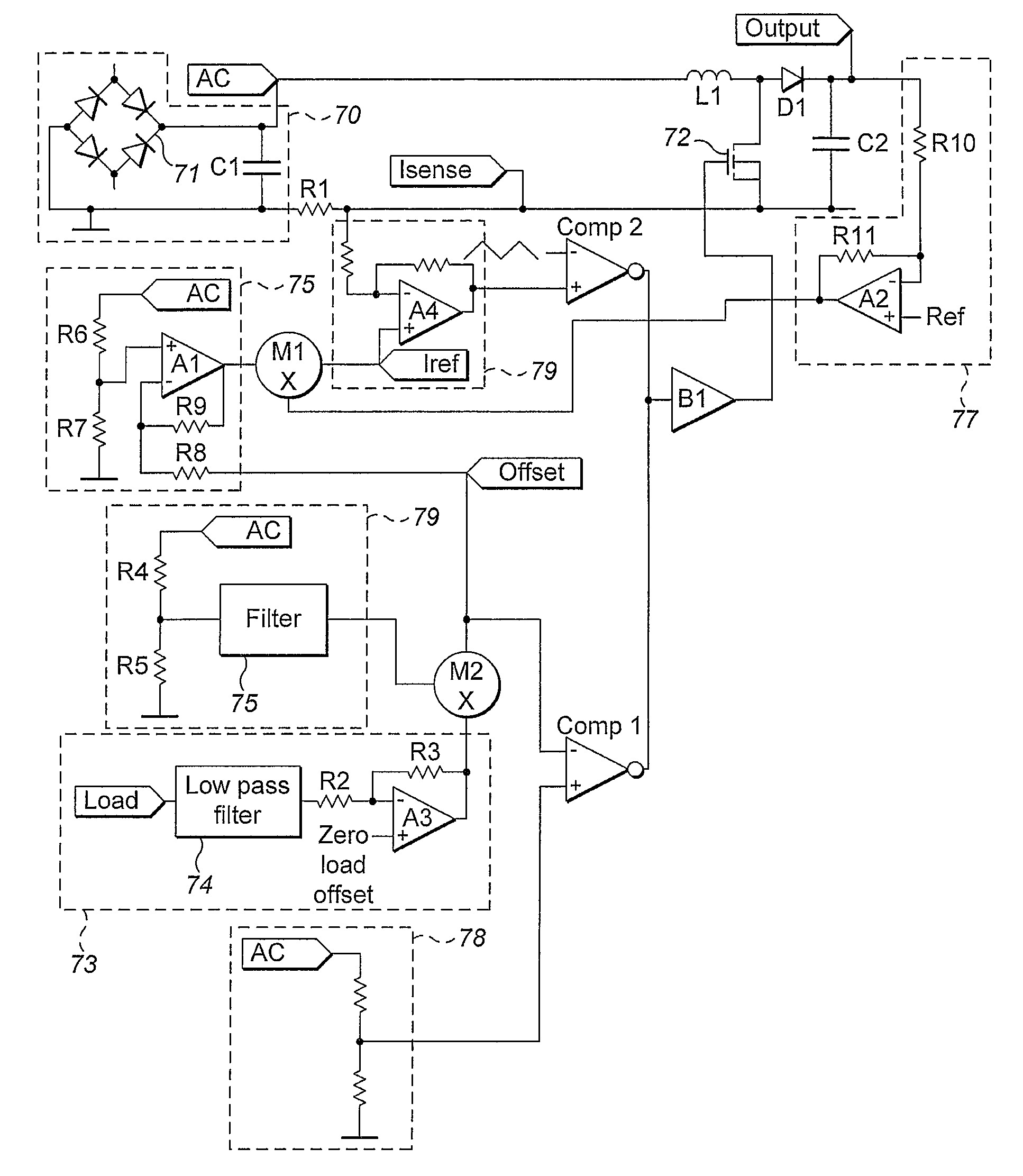
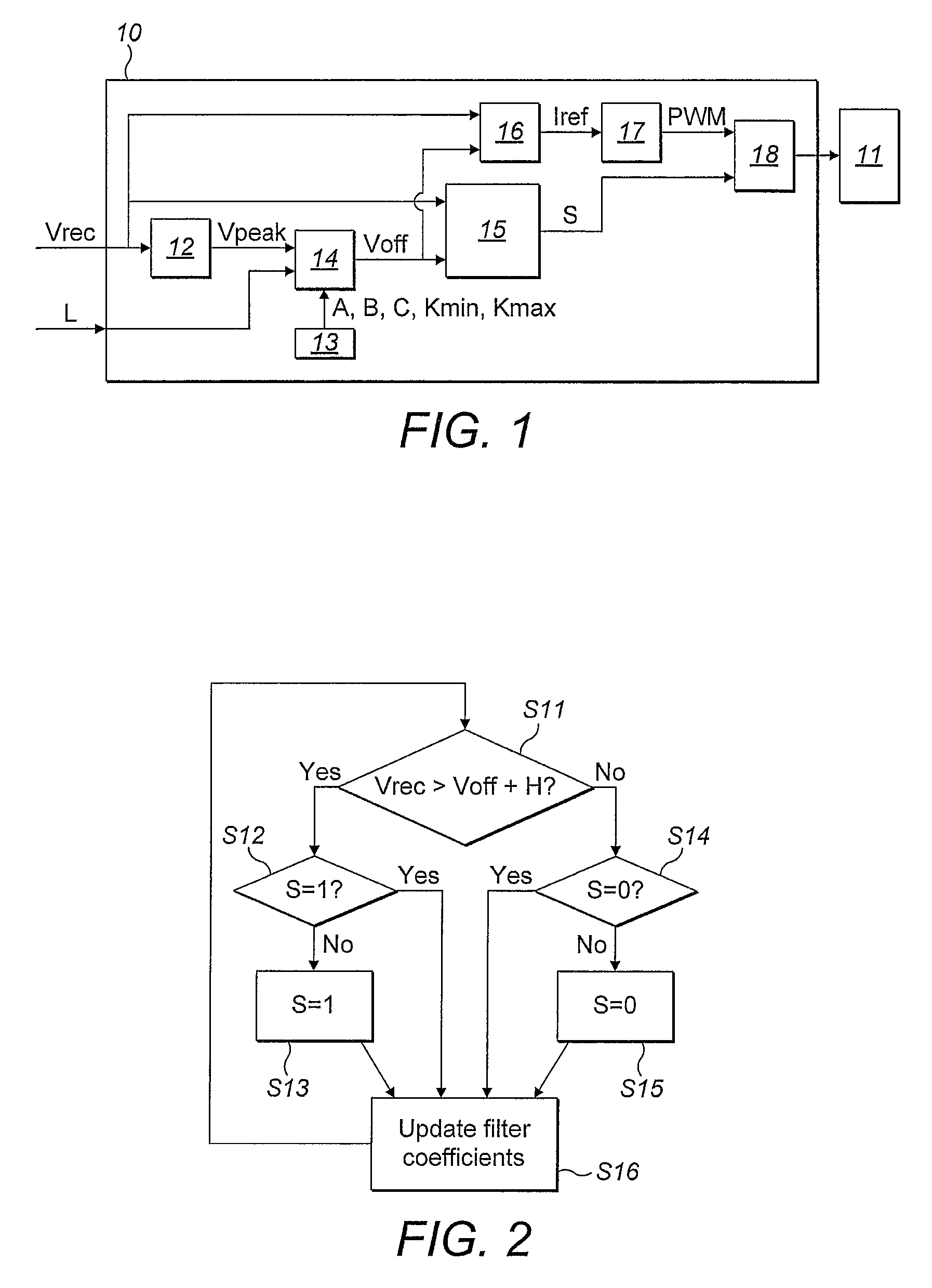
[0121]FIG. 1 shows a PFC circuit which embodies the present invention. The circuit comprises a control module 10 and a current shaping module (switching circuit) 11.

[0122]Switching circuits which shape an input current to follow the waveform of a reference signal are well known in the art. For example, a boost pre-regulator such as that described in Texas Instruments application note SLUA269. Accordingly, the components and functionality of the current shaping module 11 are not described in detail here.

[0123]A rectified voltage input Vrec is provided as an input to the control module, together with a load signal L, which represents the instantaneous current or power drawn by a load associated with the circuit.

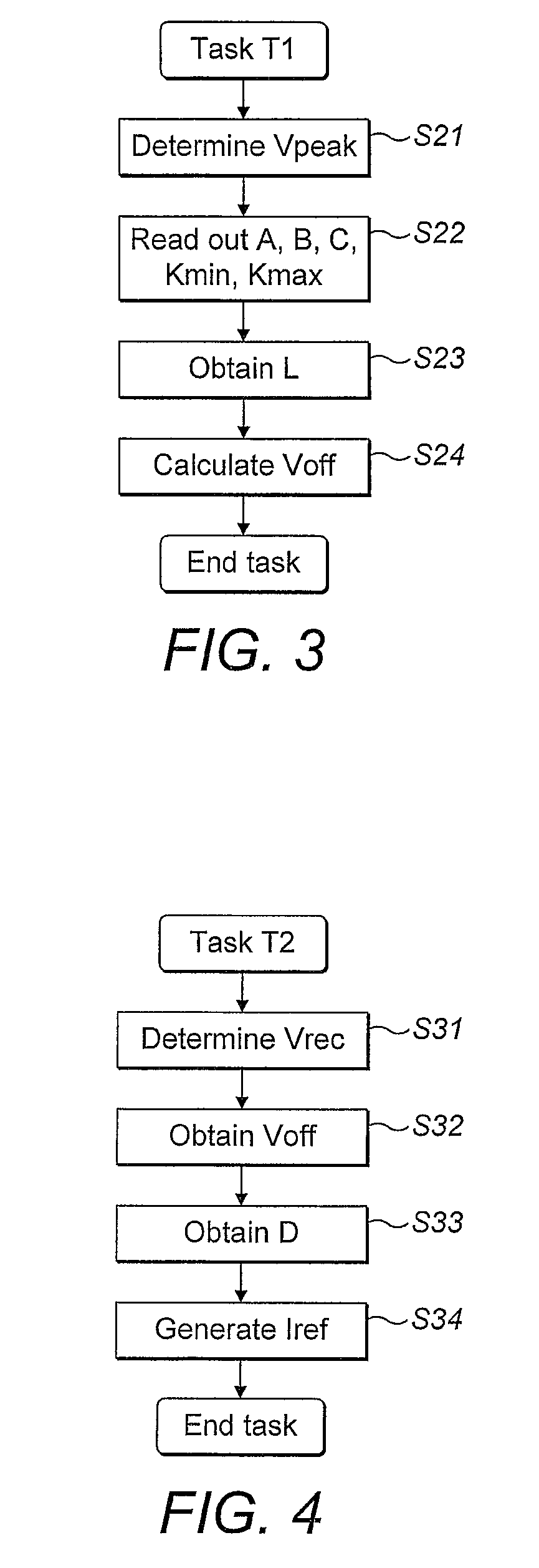
[0124]Vrec is provided as input to a first determining module 12 of the control module. The first determining module determines the peak value of Vrec, Vpeak.

[0125]The control module comprises a storage module 13. Storage module 13 stores a look-up table which comprises values ...


PUM


Abstract

Disclosed is a PFC (power factor correction) device for shaping an input current of a power converter. The device includes means for receiving a rectified input voltage derived from an AC input voltage; load determining means for determining a load value L which represents the power drawn by a load supplied by the power converter; current shaping means for shaping the input current of the power converter to follow a reference waveform; and control means for controlling the current shaping means to operate over a conduction interval α during each positive and negative half cycle of the AC input voltage. The duration of the conduction interval is controlled in accordance with the load value L. The current shaping means may shape the input current to follow the reference waveform which crosses zero at phase angles which substantially correspond to the start and end of the conduction interval.

Description

BACKGROUND OF THE INVENTION[0001]1. Field of the Invention[0002]The present invention relates to a power factor correction (PFC) device, and to power converter which incorporates a PFC device.[0003]2. Description of Related Art[0004]The requirement for loads connected to the AC mains to draw power with low harmonic distortion has existed for many years. In Europe, EN61000-3-2 is the relevant standard for single phase power supplies. EN61000-3-2 sets different limits, depending on the end equipment.[0005]For industrial applications, EN61000-3-2 defines limits in terms of absolute levels of harmonic content. In practice, power supplies which operate at up to 100 W, with a power factor of around 0.6, comply with these absolute limits without a need for additional power factor correction. However, at higher power levels, a higher power factor, close to unity, is required.[0006]For lighting and computer equipment, EN61000-3-2 defines more stringent harmonic current limits, such that a po...

Claims


Application Information

Patent Timeline
Patent Type & Authority Patents(United States)
IPC IPC(8): G05F5/00
CPCH02M1/4225Y02B70/126Y02B70/10H02M1/4208H02M3/156H02M3/33507H02M5/4585
Inventor SKINNER, ANDREW, JOHN
Owner TDK LAMBDA UK
Why Eureka
Try Eureka