Compliant and nonplanar nanostructure films

a nanostructure film, non-planar technology, applied in the direction of cell components, coatings, transportation and packaging, etc., can solve the problems of high-temperature sputtering, high-temperature sputtering, and the indium component of ito is rapidly becoming a scarce commodity, and achieves the effect of avoiding losses in structural, electrical and/or optical functionality

Active Publication Date: 2014-08-26
SAMSUNG ELECTRONICS CO LTD
View PDF8 Cites 0 Cited by
  • Summary
  • Abstract
  • Description
  • Claims
  • Application Information

AI Technical Summary

Benefits of technology

[0006]The present invention describes nanostructure films. Nanostructures have attracted a great deal of recent attention due to their exceptional material properties. Nanostructures may include, but are not limited to, nanotubes (e.g., single-walled carbon nanotubes (SWNTs), multi-walled carbon nanotubes (MWNTs), double-walled carbon nanotubes (DWNTs), few-walled carbon nanotubes (FWNTs), other fullerenes (e.g., buckyballs), graphene flakes / sheets, and / or nanowires (e.g., metallic (e.g., Ag, Ni, Pt, Au), semiconducting (e.g., InP, Si, GaN), dielectric (e.g., SiO2, TiO2), organic, inorganic). Nanostructure films may comprise at least one interpenetrating network of such nanostructures, and may similarly exhibit exceptional material properties. For example, nanostructure films comprising at least one interconnected network of carbon nanotubes (e.g., wherein nanostructure density is above a percolation threshold) can exhibit extraordinary strength and electrical conductivity, as well as efficient heat conduction and substantial optical transparency.
[0007]In one embodiment, a coated substrate may comprise a nanostructure film coated on a non-planar substrate. The substrate may be non-planar (e.g., curved, convex, concave, tubular, bent around a corner and / or edge) in a relaxed state and / or compliant, and / or may comprise a polymer (e.g., one wherein bonds begin to break at temperatures over about 150 C). The coated substrate, and / or the nanostructure film portion thereof, may be optically transparent and electrically conductive, may be bent more than 20 degrees without losses in structural, electrical and / or optical functionality, and / or may comprise an interconnected network of carbon nanotubes.

Problems solved by technology

However, ITO can be an inadequate solution for many of the above-mentioned applications (e.g., due to its relatively brittle nature, correspondingly inferior flexibility and abrasion resistance), and the indium component of ITO is rapidly becoming a scarce commodity.
Additionally, ITO deposition usually requires expensive, high-temperature sputtering, which can be incompatible with many device process flows.

Method used


Image

  • Compliant and nonplanar nanostructure films
  • Compliant and nonplanar nanostructure films
  • Compliant and nonplanar nanostructure films

Examples


Embodiment Construction

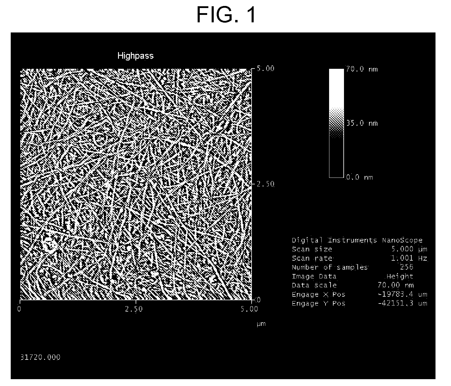
[0025]Referring to FIG. 1, a nanostructure film according to one embodiment of the present invention comprises at least one interconnected network of single-walled carbon nanotubes (SWNTs). Such film may additionally or alternatively comprise other nanotubes (e.g., MWNTs, DWNTs), other fullerenes (e.g., buckyballs), graphene flakes / sheets, and / or nanowires (e.g., metallic (e.g., Ag, Ni, Pt, Au), semiconducting (e.g., InP, Si, GaN), dielectric (e.g., SiO2, TiO2), organic, inorganic).

[0026]Such a nanostructure film may further comprise at least one functionalization material bonded to the nanostructure film. For example, a dopant bonded to the nanostructure film may increases the electrical conductivity of the film by increasing carrier concentration. Such dopant may comprise at least one of Iodine (I2), Bromine (Br2), polymer-supported Bromine (Br2), Antimonypentafluride (SbF5), Phosphoruspentachloride (PCl5), Vanadiumoxytrifluride (VOF3), Silver(II)Fluoride (AgF2), 2,1,3-Benzoxadiaz...


PUM

PropertyMeasurementUnit
semi-transparentaaaaaaaaaa
poweraaaaaaaaaa
transparencyaaaaaaaaaa

Abstract

A coated substrate comprising a nanostructure film formed on a non-planar substrate is described. The coated substrate may further be compliant, optically transparent and / or electrically conductive. Fabrication methods thereof are also described.

Description

[0001]This application claims priority to U.S. Provisional Patent Application Nos. 60 / 829,470, filed Oct. 13, 2006 and entitled “FLASH-DRY DEPOSITION OF NANOSTRUCTURE FILMS,” and 60 / 865,826, filed Nov. 14, 2006 and entitled “TRANSFER STAMPING OF NANOSTRUCTURE FILMS.”FIELD OF THE INVENTION[0002]The present invention relates generally to nanostructure films and / or deposition methods thereof, and more specifically to non-planar and compliant nanostructure films and / or deposition methods thereof.BACKGROUND OF THE INVENTION[0003]Many modern and / or emerging applications require at least one device electrode that has not only high electrical conductivity, but high optical transparency as well. Such applications include, but are not limited to, touch screens (e.g., analog, resistive, 4-wire resistive, 5-wire resistive, surface capacitive, projected capacitive, multi-touch, etc.), displays (e.g., flexible, rigid, electro-phoretic, electro-luminescent, electrochromatic, liquid crystal (LCD), ...

Claims


Application Information

Patent Timeline
Patent Type & Authority Patents(United States)
IPC IPC(8): B05D5/12C08J7/043C08J7/044
CPCH01B1/24B05D1/286C08J7/06C08J2367/02H01M4/366Y02E60/10C08J7/043C08J7/044Y10T428/13Y10T428/24
Inventor HU, LIANGBINGHECHT, DAVIDJUE, JEFFREYGRUNER, GEORGE
Owner SAMSUNG ELECTRONICS CO LTD
Why Eureka
Try Eureka