

Nitride semiconductor device using selective growth and manufacturing method thereof
a semiconductor device and selective growth technology, applied in the direction of semiconductor devices, basic electric elements, electrical appliances, etc., can solve the problems of significant affecting the switch characteristics of the device, and achieve the effect of reducing or eliminating a leakage current and improving the breakdown voltage characteristics
- Summary
- Abstract
- Description
- Claims
- Application Information
AI Technical Summary
Benefits of technology
Problems solved by technology
Method used
Image

Examples
first embodiment
[0074
[0075]A first embodiment disclosed in the present disclosure may be implemented by a portion or combination of the components or steps included in the foregoing embodiments or may be implemented by a combination of the embodiments. Hereinafter, repeated portions may be omitted for clarity of the first embodiment of the present disclosure.
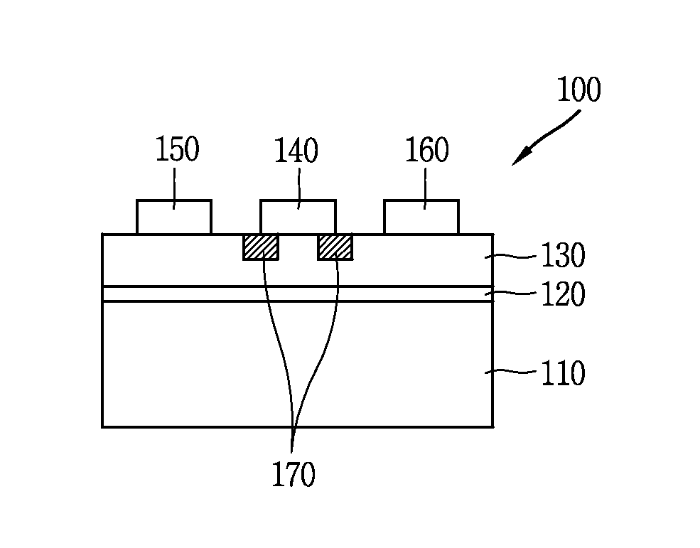
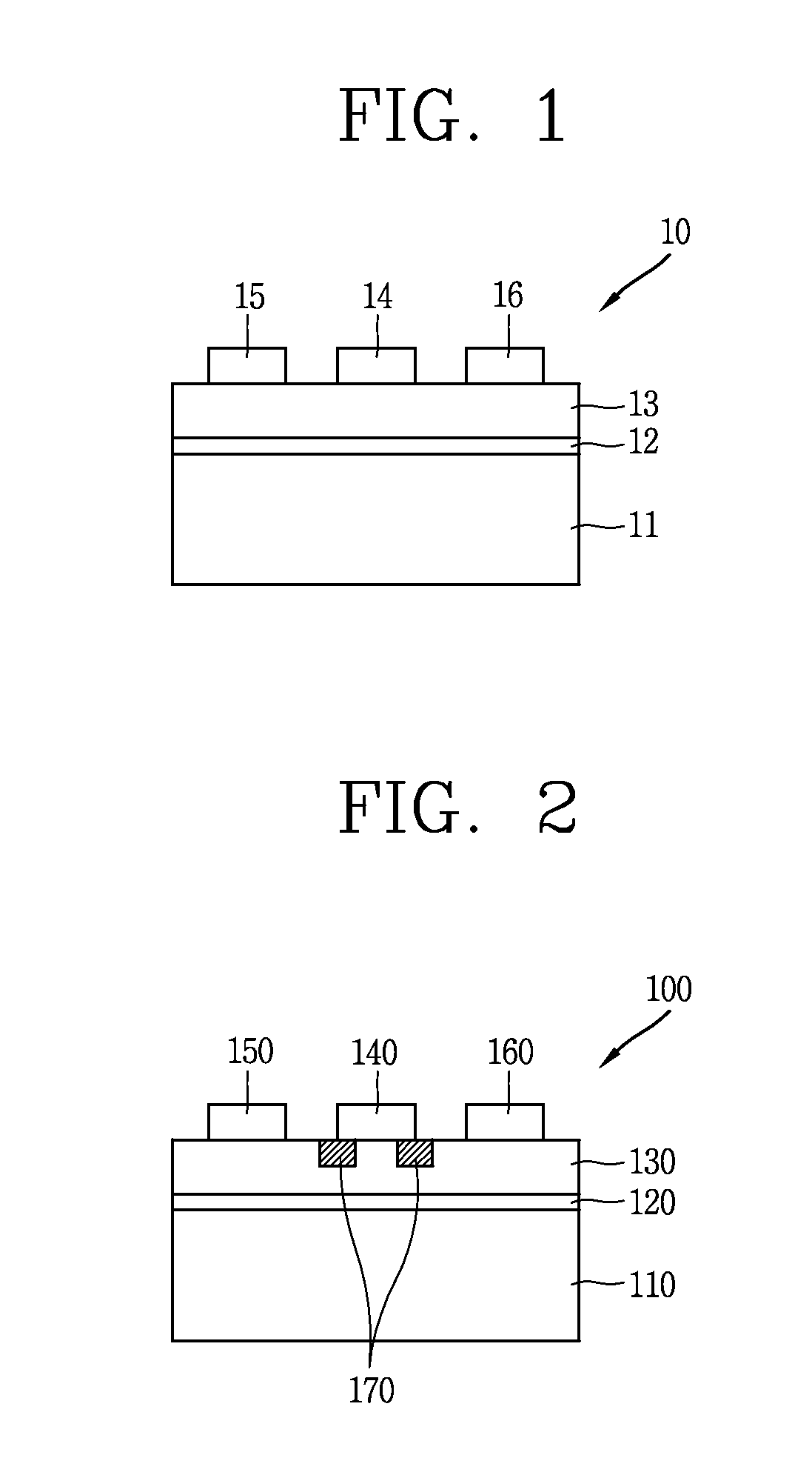
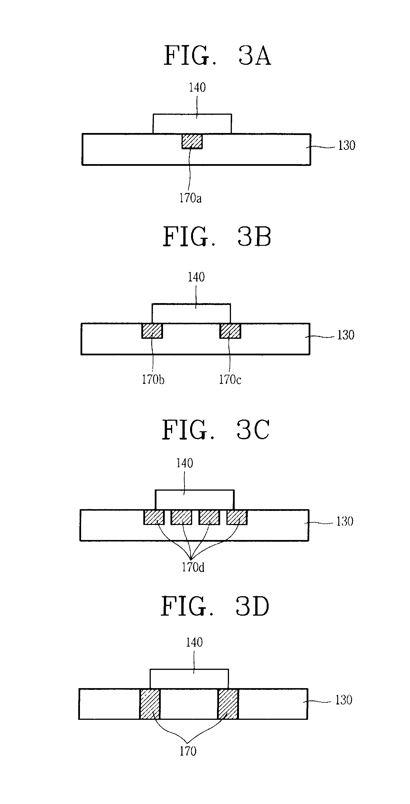
[0076]A semiconductor device according to a first embodiment of the present invention may include a substrate, a first GaN layer formed on the substrate, an AlGaN layer formed on the first GaN layer, a second GaN layer formed on the AlGaN layer and including a p type GaN layer, and a gate electrode formed on the second GaN layer, wherein the p type GaN layer may be in contact with a portion of the gate electrode.
[0077]Also, according to the first embodiment of the present disclosure, the second GaN layer may have a recess, and the p type GaN layer may be formed on the recess.
[0078]Also, according to the first embodiment of the present disclosur...
second embodiment
[0088
[0089]A second embodiment disclosed in the present disclosure may be implemented by a portion or combination of the components or steps included in the foregoing embodiments or may be implemented by a combination of the embodiments. Hereinafter, repeated portions may be omitted for clarity of the second embodiment of the present disclosure.
[0090]A semiconductor device according to a second embodiment of the present invention may include a substrate, a first GaN layer formed on the substrate, an AlGaN layer formed on the first GaN layer, a second GaN layer formed on the AlGaN layer and including a p type GaN layer, and a gate electrode formed on the second GaN layer, wherein the p type GaN layer may be in contact with a portion of the gate electrode.
[0091]Also, according to the second embodiment of the present disclosure, the second GaN layer may have a recess, and the p type GaN layer may be formed on the recess.
[0092]Also, according to the second embodiment of the present disc...
PUM
 Abstract
Description
Claims
Application Information