Light-emitting element

a technology of light-emitting elements and light-emitting elements, which is applied in the field of light-emitting elements, can solve the problems of insufficient utilization of energy transfer from the singlet excited state of the host molecule to the guest molecule, and achieve the effects of suppressing the reverse energy transfer, high-efficiency light-emitting element, and high-efficiency light-emitting elemen

Active Publication Date: 2014-10-07
SEMICON ENERGY LAB CO LTD
View PDF129 Cites 124 Cited by
  • Summary
  • Abstract
  • Description
  • Claims
  • Application Information

AI Technical Summary

Benefits of technology

[0031]Phosphorescent organometallic complexes (e.g., iridium complexes) used as a phosphorescent guest molecule generally have an absorption originating from the triplet MLCT (metal-to-ligand charge transfer) transition in a relatively long wavelength region. Their excitation spectra suggest that this absorption in a long wavelength region (mainly located at around 450 nm) significantly contributes to the emission of the guest molecule. Hence, it is preferable that this absorption in a long wavelength region fairly overlaps with the phosphorescent spectra of the host molecule. This is because such a large overlapping allows the energy transfer from the triplex exited state of the host molecule to efficiently take place, resulting in an efficient formation of the triplet excited state of the guest molecule.
[0033]That is, the traditional phosphorescent light-emitting elements have a quite low probability that the energy transfer from the singlet excited state of the host molecule to the phosphorescent guest molecule occurs to form the singlet excited state of the guest molecule which is subsequently transformed to the triplet excited state by the intersystem crossing.
[0034]The present invention is made in view of these problems, and one embodiment of the present invention provides a light-emitting element based on a novel principle. In addition, one embodiment of the present invention provides a light-emitting element having high external quantum efficiency.
[0037]It is considered that exciplexes have a small energy difference between the singlet excitation energy and the triplet excitation energy. In other words, the an emission from the singlet excited state and that from the triplet excited state appear in wavelength regions which are very close to each other. Additionally, because emission of exciplexes is usually observed in a longer wavelength region than that of their monomer states, it is possible to increase the overlapping between the absorptions of phosphorescent compounds, which appear in a long wavelength region and originate from the triplet MLCT transition, and the emission of the exciplexes. This means that energy can be efficiently transferred from both of the singlet and triplet states of exciplexes to phosphorescent compounds, which contributes to the improvement in the efficiency of the light-emitting elements.
[0046]In contrast, in the case where the n-type host and the p-type host can form an exciplex, the guest molecules can be excited also through the process of energy transfer from the singlet and triplet states of the exciplex to the guest molecules as mentioned above, which enables an increase in the emission efficiency compared with the traditional phosphorescent light-emitting elements.
[0048]In any of the above embodiments, the interface between the light-emitting layer containing a mixture of the n-type host and the p-type host and the n-type host layer serves as a barrier to holes, but hardly serves as an obstacle to electrons. The interface between the light-emitting layer and the p-type host layer serves as a barrier to electrons, but hardly serves as an obstacle to holes. Therefore, electrons and holes are confined in the light-emitting layer or between the n-type host layer and the p-type host layer. As a result, electrons and holes can be prevented from reaching an anode and a cathode, respectively, whereby emission efficiency can be improved. In general, exciplexes provide broad emission spectra. On the other hand, since the guest molecule emits light in the embodiments of the present invention, emission spectra with a small half width can be obtained, which allows the formation of a light-emitting element that is capable of emitting light with excellent color purity.Reference

Problems solved by technology

Therefore, it is impossible to sufficiently utilize the energy transfer from the singlet excited state of the host molecule to the guest molecule.

Method used


Image

  • Light-emitting element
  • Light-emitting element
  • Light-emitting element

Examples


embodiment 1

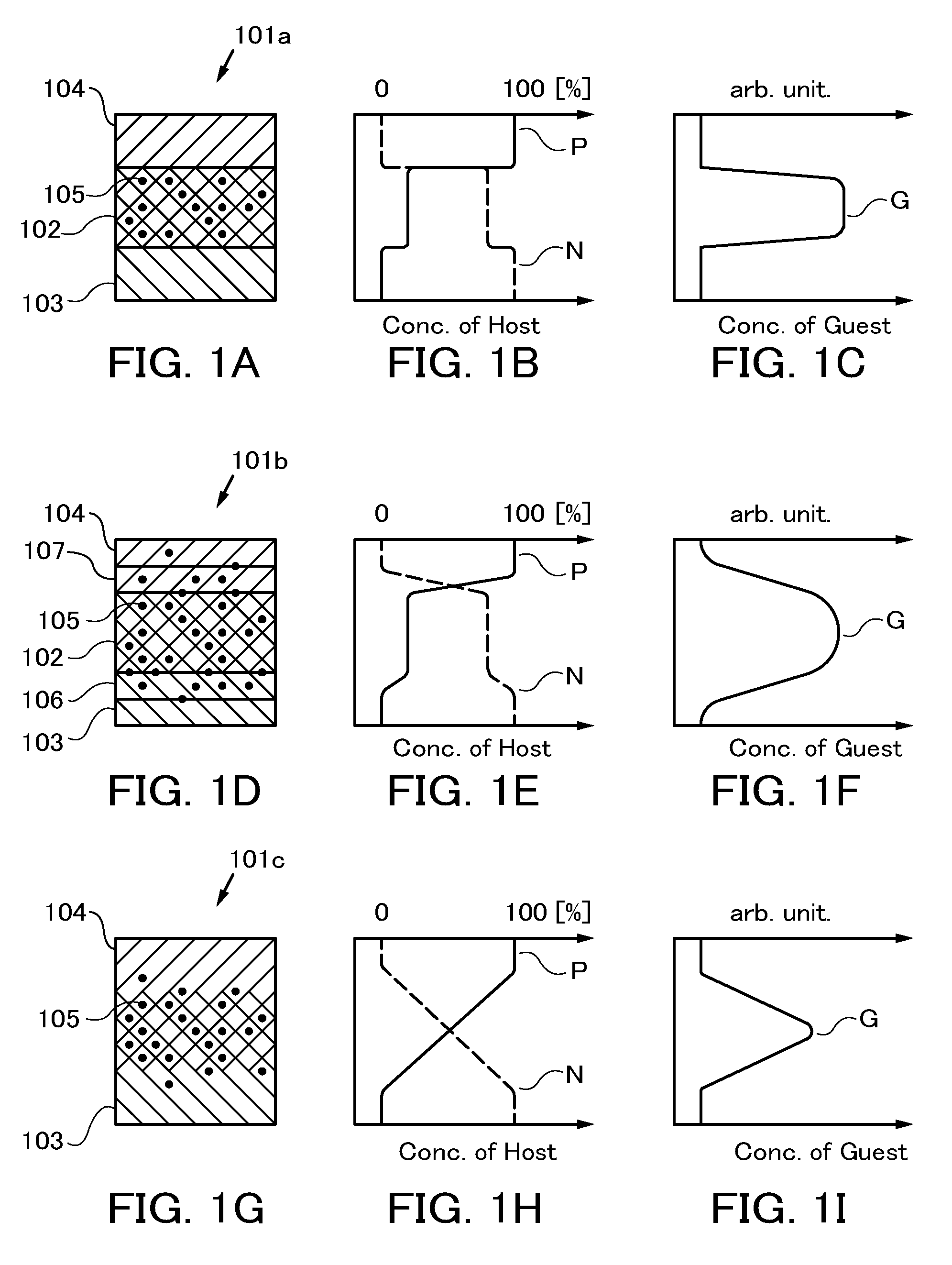
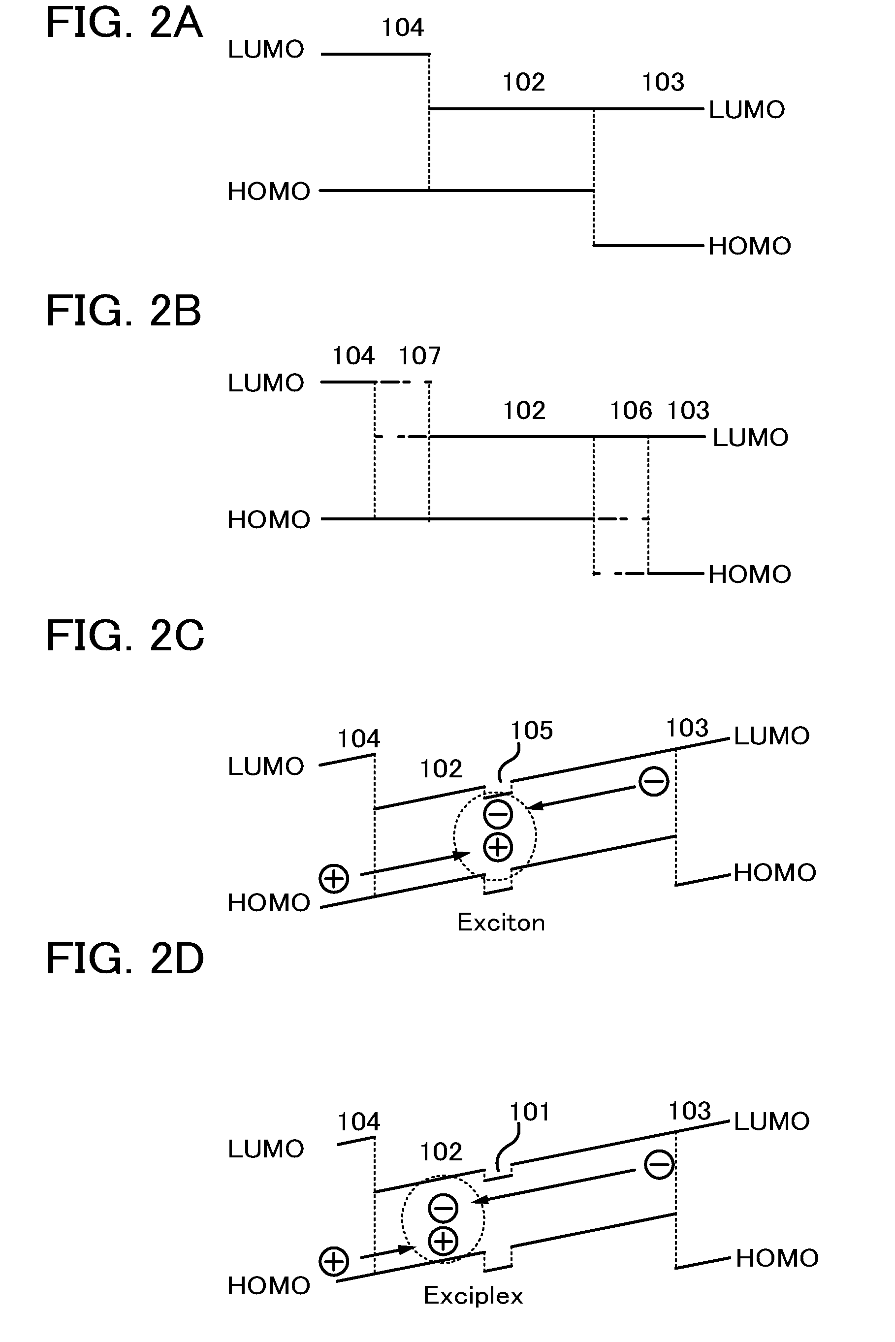
[0059]A light-emitting element 101a which is an example in this embodiment includes an n-type host layer 103 including an n-type host, a p-type host layer 104 including a p-type host, and a layer containing both the n-type host and the p-type host (hereinafter referred to as a light-emitting layer 102) interposed therebetween, as illustrated in FIG. 1A. Guest molecules 105 are dispersed in the light-emitting layer 102.

[0060]FIG. 1B illustrates distributions of the concentration of the n-type host (denoted by “N” in the diagram) and the concentration of the p-type host (denoted by “P” in the diagram) in the light-emitting element 101a. In the light-emitting layer 102 of the light-emitting element 101a, the concentration of the n-type host is 80% and the concentration of the p-type host is 20%. In other words, in the light-emitting layer 102, the ratio of the n-type host to the p-type host is 4:1. This ratio may be determined in consideration of the transport properties of the n-type ...

embodiment 2

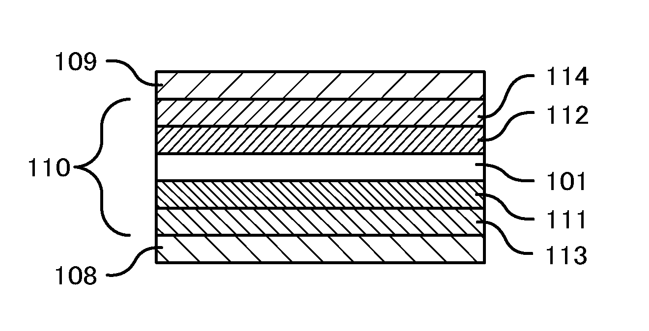
[0102]FIG. 3A illustrates an example of a light-emitting device of this embodiment. The light-emitting device illustrated in FIG. 3A is that in which a light-emitting element 101 described in Embodiment 1 (such as the light-emitting element 101a, the light-emitting element 101b, or the light-emitting element 101c described in Embodiment 1) is sandwiched between a cathode 108 and an anode 109. Note that at least one of the cathode 108 and the anode 109 is preferably transparent. This light-emitting device may be provided over an appropriate substrate.

[0103]In the light-emitting element 101, the n-type host layer 103 and the p-type host layer 104 between which the light-emitting layer 102 is sandwiched function as an electron-transport layer and a hole-transport layer, respectively, and function to block holes and electrons, respectively, as described above. Thus, layers corresponding to an electron-transport layer and a hole-transport layer do not need to be additionally provided. Ac...

embodiment 3

[0168]In this embodiment, apparatuses and methods for manufacturing the light-emitting element 101a or the like described in Embodiment 1 will be described. A manufacturing apparatus illustrated in FIG. 4A includes a first evaporation source 202, a second evaporation source 203, and a third evaporation source 204 in a vacuum chamber 201. The first to third evaporation sources 202 to 204 each have a linear opening portion 223 as illustrated in FIG. 4C and allows an inside organic compound to evaporate by a resistance heating method.

[0169]Here, the first evaporation source 202, the second evaporation source 203, and the third evaporation source 204 cause the n-type host, the guest, and the p-type host to evaporate, respectively. The first to third evaporation sources 202 to 204 may each be provided with a shutter. Furthermore, it is preferable that the temperatures of the evaporation sources can be controlled independently so that the vapor pressures of the organic compounds can be co...


PUM


Abstract

A light-emitting element having extremely high efficiency of approximately 25% is provided. The light-emitting element includes a light-emitting layer which contains a phosphorescent guest, an n-type host, and a p-type host, where the light-emitting layer is interposed between an n-type layer including the n-type host and a p-type layer including the p-type host, and where the n-type host and the p-type host are able to form an exciplex in the light-emitting layer. The light-emitting element exhibits an extremely high emission efficiency (power efficiency of 74.3 lm / W, external quantum efficiency of 24.5%, energy efficiency of 19.3%) at a low driving voltage (2.6 V) at which luminance of 1200 cd / m2 is attainable.

Description

TECHNICAL FIELD[0001]The present invention relates to light-emitting elements using an organic electroluminescence (EL) phenomenon (hereinafter such light-emitting elements are also referred to as organic EL elements).BACKGROUND ART[0002]Organic EL elements have been actively researched and developed. In a fundamental structure of the organic EL element, a layer including a luminescent organic compound (hereinafter also referred to as light-emitting layer) is interposed between a pair of electrodes. The organic EL element has attracted attention as a next-generation flat panel display element owing to characteristics such as feasibility of being thinner and lighter, high speed response to input signals, and capability of direct current low voltage driving. In addition, a display using such a light-emitting element has a feature that it is excellent in contrast and image quality, and has a wide viewing angle. Further, being a planar light source, the organic EL element has been attem...

Claims


Application Information

Patent Timeline
Patent Type & Authority Patents(United States)
IPC IPC(8): H01L29/08H01L21/00H01L27/32H01L51/00H01L51/50
CPCH01L51/5016H01L51/0074H01L2251/5384H01L2251/5346H01L27/3209H01L51/0059H01L51/0072H01L51/0071H01L51/5056H01L51/504H01L51/5072H01L51/0061H01L51/0085H01L2251/5376H10K59/32H10K85/00H10K85/631H10K85/6576H10K85/6572H10K85/657H10K50/11H10K50/00H10K2101/10H10K2101/80H10K2101/90H10K50/805H10K50/13H10K85/342H10K85/636H10K50/15H10K50/16H10K2101/27
Inventor YAMAZAKI, SHUNPEISEO, SATOSHISHITAGAKI, SATOKOOHSAWA, NOBUHARUINOUE, HIDEKOKADOMA, HIROSHIOSAKA, HARUE
Owner SEMICON ENERGY LAB CO LTD
Why Eureka
Try Eureka