Circuit and system of a low density one-time programmable memory

a one-time programmable memory and circuit technology, applied in the field of circuits and systems of low density one-time programmable memory, can solve the problems of ineffective counter and flip-flop according to the conventional design, large cell size of electrical fuse using silicided polysilicon, etc., to reduce otp memory size, low density otps, and save cost

Inactive Publication Date: 2014-10-14
ATTOPSEMI TECH CO LTD
View PDF139 Cites 55 Cited by
  • Summary
  • Abstract
  • Description
  • Claims
  • Application Information

AI Technical Summary

Benefits of technology

[0009]The present invention relates to effective circuit and system designs for testing a one-time-programmable (OTP) memory. Embodiments of highly effective circuits and systems for low density OTPs are disclosed. Inventions to replace the conventional counters and flip-flop designs can greatly reduce OTP memory size and save cost.

Problems solved by technology

As a result, the cell size of an electrical fuse using silicided polysilicon tends to be very large.
The counter and flip-flop according to the conventional designs are very ineffective.

Method used


Image

  • Circuit and system of a low density one-time programmable memory
  • Circuit and system of a low density one-time programmable memory
  • Circuit and system of a low density one-time programmable memory

Examples


Embodiment Construction

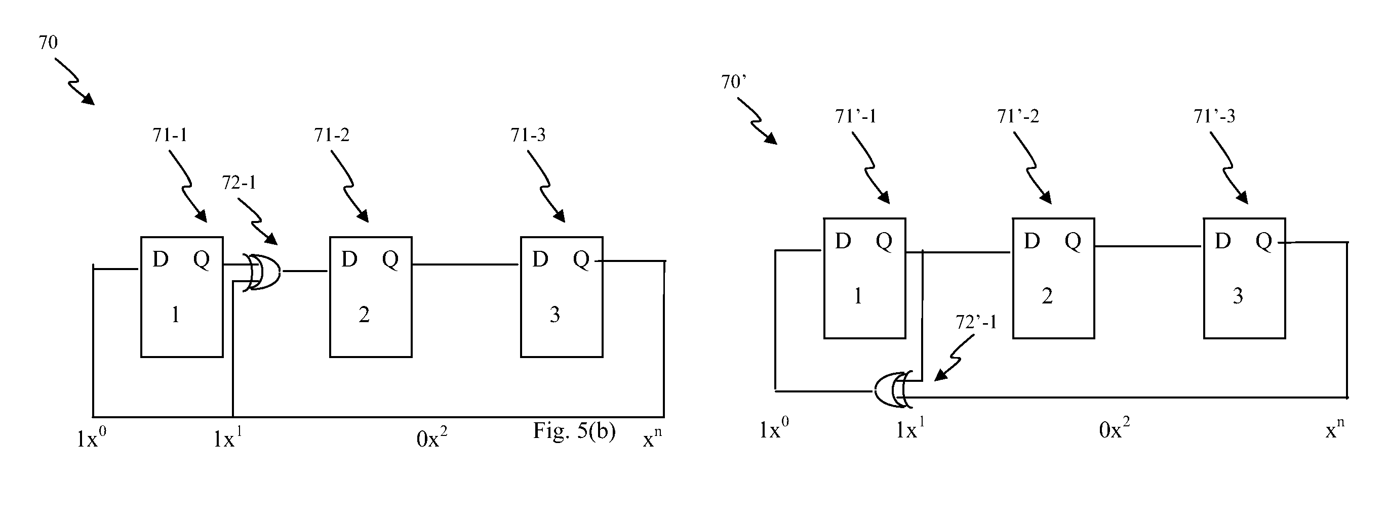
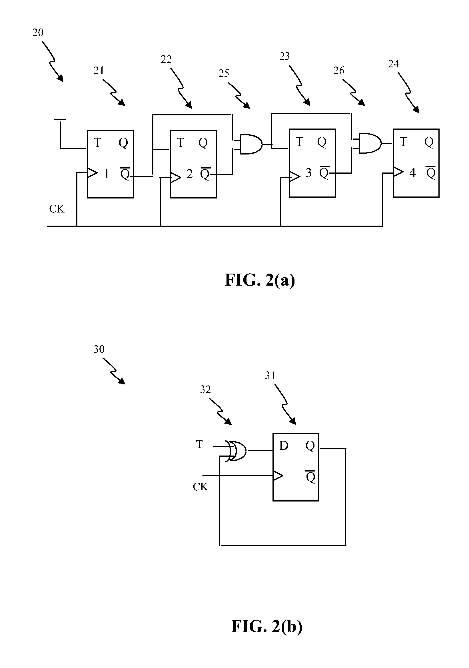
[0035]Embodiments disclosed herein use innovations to reduce gate counts for a low density OTP memory. A counter with high gate count is replaced by a Linear Feedback Shift Register (LFSR) to generate addresses in a serial OTP memory. LFSR can generate almost the entire available address spaces with a proper design, except the all 0s state. The all 0s state can be multiplexed in and out at any time to reach the entire 2n address spaces, the same effect as a counter, except that the addresses are not generated incremented or decremented but in a seemingly pseudo-random manner. Either counter or LFSR can be designed based on D-type flip-flops (DFFs). The conventional design for DFFs is based on pass gates to drive a pair of cross-coupled inverters that needs about 24 transistors (24T). A better DFF can be designed with two latches. Each latch has a pair of cross-coupled inverters as two outputs coupled to drains of a pair of NMOS input devices. The gates of the NMOS input devices are ...


PUM


Abstract

A low density One-Time Programmable (OTP) memory is disclosed to achieve low gate count and low overhead in the peripheral circuits to save the cost. A maximum-length Linear Feedback Shift Register (LFSR) can be used to generate 2n−1 address spaces from an n-bit address. The registers used in the address generator can have two latches. Each latch has two cross-coupled inverters with two outputs coupled to the drains of two MOS input devices, respectively. The inputs of the latch are coupled to the gates of the MOS input devices, respectively. The sources of the MOS input devices are coupled to the drains of at least one MOS device(s), whose gate(s) are coupled to a clock signal and whose source(s) are coupled to a supply voltage. The two latches can be constructed in serial with the outputs of the first latch coupled to the inputs of the second latch.

Description

CROSS-REFERENCE TO RELATED APPLICATION[0001]This application claims priority benefit of an U.S. Provisional Application No. 61 / 595,171, filed on Feb. 6, 2012 and entitled “CIRCUIT AND SYSTEM OF A LOW DENSITY ONE-TIME PROGRAMMABLE MEMORY,” which is hereby incorporated herein by reference.BACKGROUND OF THE INVENTION[0002]One-Time Programmable (OTP) memory is a memory that can be programmed once and only once. An OTP can be programmed from low to high resistance states, the so-called fuse, such as electrical fuse. Alternatively, an OTP can be programmed from high to low resistance states, the so-called anti-fuse. The programming means can apply a high voltage to an OTP element such as in anti-fuse. Alternatively, the programming means can apply a high current to flow through an OTP element such as in fuse. The OTP memory cell usually has a program selector coupled to an OTP element to switch the desirable OTP element to conduct a high current or high voltage applied.[0003]An electrical...

Claims


Application Information

Patent Timeline
Patent Type & Authority Patents(United States)
IPC IPC(8): G11C8/00G11C17/16G11C27/04G11C8/18G11C11/16G11C17/08G11C17/12G11C17/18G11C19/28H03K3/00H03K3/356
CPCG11C11/1659G11C27/04H03K3/00G11C8/18G11C17/16G11C17/18G11C11/1675H03K3/35606G11C17/12G11C19/28G11C17/08
Inventor CHUNG, SHINE, C.
Owner ATTOPSEMI TECH CO LTD
Why Eureka
Try Eureka