
Graphene and power storage device, and manufacturing method thereof

a technology which is applied in the field of graphene and power storage devices, can solve the problems of difficult to increase the charge and discharge capacity per unit weight or volume of the electrode, the electrode is likely to be deformed and broken, and the effect of high conductivity

Active Publication Date: 2014-11-11
SEMICON ENERGY LAB CO LTD
View PDF114 Cites 37 Cited by
  • Summary
  • Abstract
  • Description
  • Claims
  • Application Information

AI Technical Summary

Benefits of technology

The present invention provides a power storage device with high charge and discharge capacity per unit weight or volume of an electrode, high reliability, and durability. The device includes a layer of graphene formed through a method that involves forming a layer of graphene oxide over a first conductive layer and reducing the oxide to graphene using a potential range of 1.4 V to 2.6 V. The resulting graphene has a higher proportion of C(sp2)-C(sp2) double bonds and higher conductivity than graphene formed through heat treatment. The invention also provides a manufacturing method for the power storage device.

Problems solved by technology

For this reason, it is difficult to efficiently increase only the weight of the active material in an electrode, and thus, it is difficult to increase the charge and discharge capacity per unit weight or volume of the electrode.
Further, the conventional electrode also has a problem in that the binder included in the active material layer swells as it comes into contact with an electrolyte, so that the electrode is likely to be deformed and broken.

Method used


Image

  • Graphene and power storage device, and manufacturing method thereof
  • Graphene and power storage device, and manufacturing method thereof
  • Graphene and power storage device, and manufacturing method thereof

Examples


embodiment 1

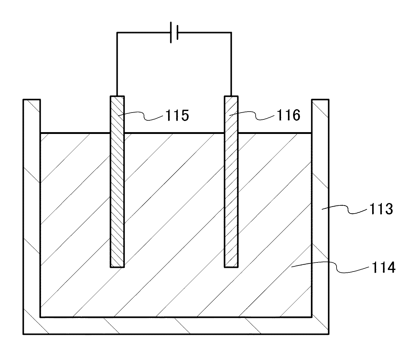
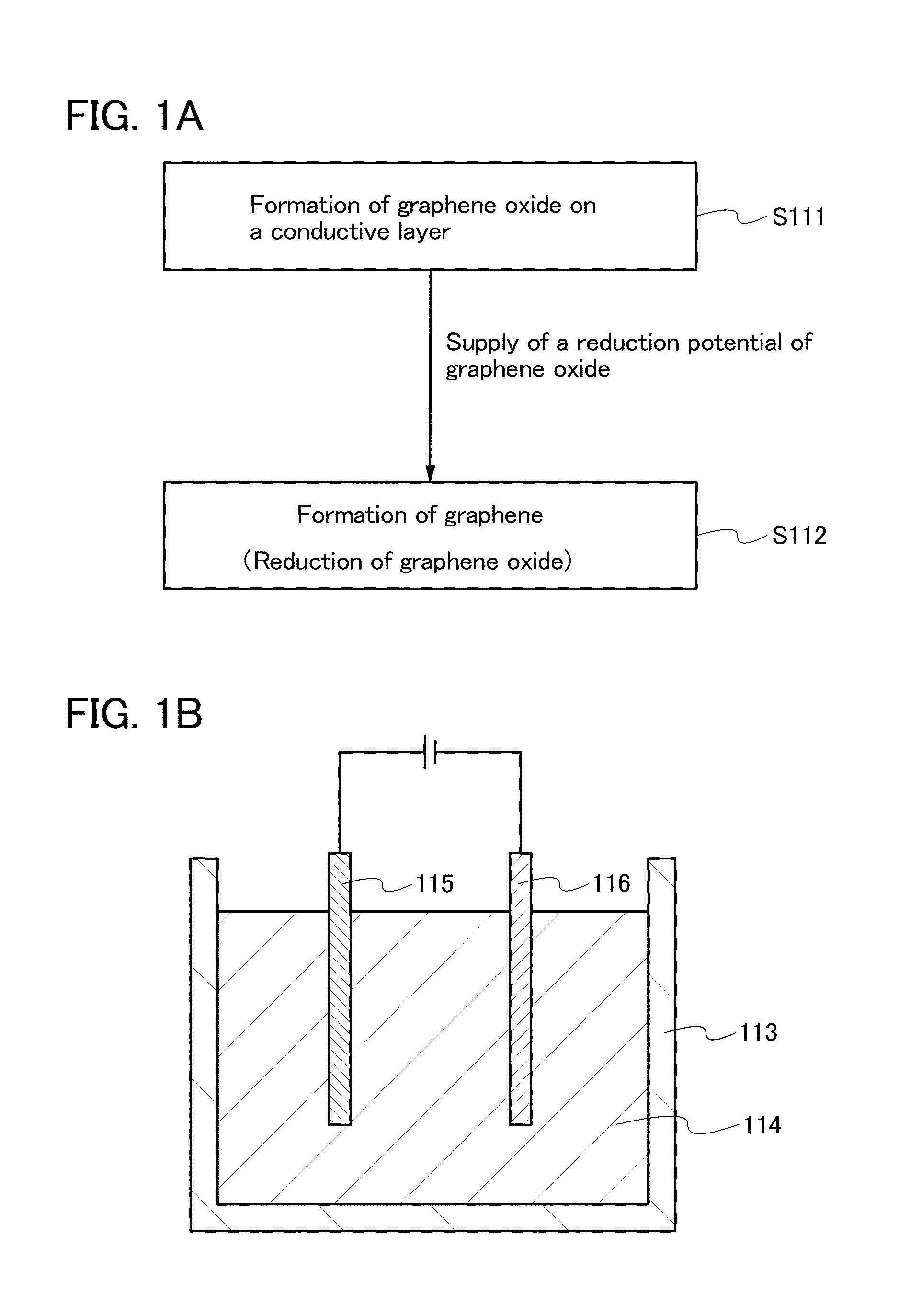
[0041]In this embodiment, a method for forming graphene of one embodiment of the present invention will be described below with reference to FIGS. 1A and 1B. FIG. 1A is a flow chart showing a process of forming graphene, and FIG. 1B is a schematic view of an apparatus used to form graphene.

[0042]According to the method for forming graphene of one embodiment of the present invention, to form graphene, graphene oxide is not reduced through heat treatment but electrochemically reduced with electric energy.

111>

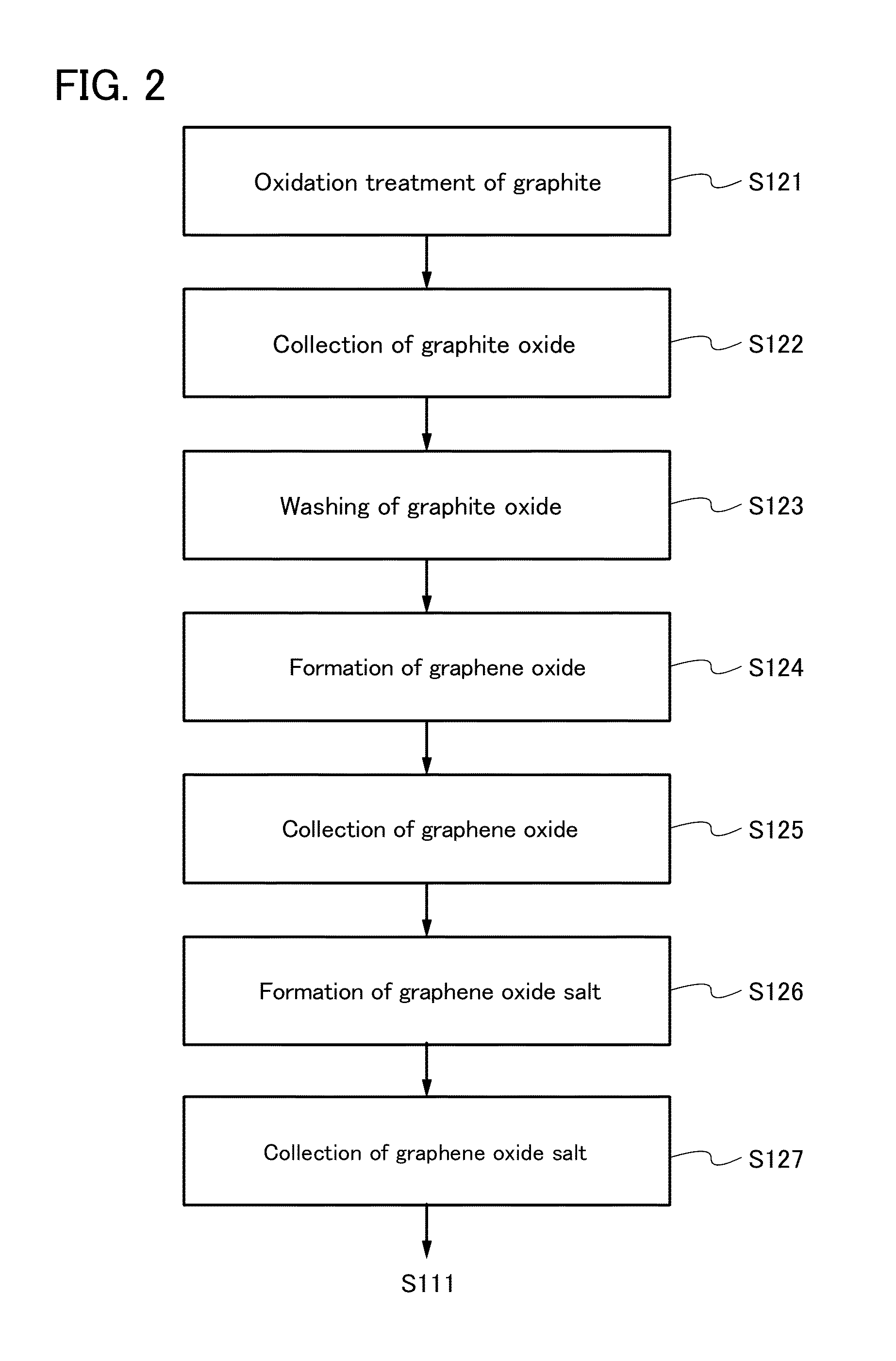
[0043]In Step S111 shown in FIG. 1A, a layer including graphene oxide is formed on a surface of a conductive layer. For example, a dispersion liquid containing graphene oxide is applied to the conductive layer. As the dispersion liquid containing graphene oxide, a commercial product or a dispersion liquid obtained by dispersing graphene oxide formed by the method described with reference to FIG. 14, or the like, in a solvent may be used. Alternatively, a dispersion liquid obtained...

embodiment 2

[0082]In this embodiment, a power storage device of one embodiment of the present invention will be described. Specifically, a power storage device including an electrode formed by the formation method of graphene, which is described in Embodiment 1, will be described. Note that in this embodiment, description will be given assuming that the power storage device of one embodiment of the present invention is a lithium secondary battery.

[0083]First, a positive electrode 311 will be described.

[0084]FIG. 4A is a cross-sectional view of a positive electrode 311. In the positive electrode 311, a positive electrode active material layer 309 is formed over a positive electrode current collector 307. The positive electrode active material layer 309 includes at least a positive electrode active material 321 and graphene 323 (not illustrated) and may further include binder, a conductive additive, and / or the like.

[0085]Note that an active material refers to a material that relates to insertion ...

embodiment 3

[0161]The power storage device of one embodiment of the present invention can be used for power supplies of a variety of electric appliances which can be operated with electric power.

[0162]Specific examples of electric appliances each utilizing the power storage device of one embodiment of the present invention are as follows: display devices, lighting devices, desktop personal computers and laptop personal computers, image reproduction devices which reproduce still images and moving images stored in recording media such as digital versatile discs (DVDs), mobile phones, portable game machines, portable information terminals, e-book readers, video cameras, digital still cameras, high-frequency heating appliances such as microwave ovens, electric rice cookers, electric washing machines, air-conditioning systems such as air conditioners, electric refrigerators, electric freezers, electric refrigerator-freezers, freezers for preserving DNA, and dialyzers. In addition, moving objects dri...


PUM

PropertyMeasurementUnit
temperatureaaaaaaaaaa
thicknessaaaaaaaaaa
sizeaaaaaaaaaa

Abstract

The formation method of graphene includes the steps of forming a layer including graphene oxide over a first conductive layer; and supplying a potential at which the reduction reaction of the graphene oxide occurs to the first conductive layer in an electrolyte where the first conductive layer as a working electrode and a second conductive layer with a as a counter electrode are immersed. A manufacturing method of a power storage device including at least a positive electrode, a negative electrode, an electrolyte, and a separator includes a step of forming graphene for an active material layer of one of or both the positive electrode and the negative electrode by the formation method.

Description

TECHNICAL FIELD[0001]The present invention relates to formation methods of graphene and an electrode including the graphene, and a manufacturing method of a power storage device including the electrode. The present invention also relates to graphene and an electrode which are formed by the formation methods and a power storage device which is manufactured by the manufacturing method. Note that a power storage device in this specification refers to every element and / or device having a function of storing electric power, such as a lithium primary battery, a lithium secondary battery, or a lithium-ion capacitor.BACKGROUND ART[0002]In recent years, attempts have been made to apply graphene to a variety of products because of its excellent electric characteristic of high conductivity and its excellent physical characteristics such as sufficient flexibility and high mechanical strength.[0003]Application of graphene to power storage devices such as a lithium secondary battery and a lithium...

Claims


Application Information

Patent Timeline
Patent Type & Authority Patents(United States)
IPC IPC(8): H01M10/0566C01B31/04H01M4/139H01M6/16H01M4/62H01M4/583H01G9/042H01M4/04H01G11/32H01G11/22
CPCH01M4/583H01M4/62B82Y40/00H01M4/133H01M4/1393H01M4/0452Y02E60/122Y02E60/13H01G11/22H01M6/16H01M4/0438H01M4/587H01M10/0525H01G11/32B82Y30/00H01M4/139H01G9/042H01M10/0566C01B31/0476H01G11/36H01M4/5835C01B31/043C01B32/192C01B32/23Y02E60/10Y02T10/70Y02P70/50H01M10/052H01M4/625H01M4/386H01M4/5825H01M4/505H01M4/525
Inventor TODORIKI, HIROATSUSAITO, YUMIKOKAWAKAMI, TAKAHIRONOMOTO, KUNIHARUYUKAWA, MIKIO
Owner SEMICON ENERGY LAB CO LTD
Learn More