Active device and active device array substrate
a technology of active devices and array substrates, which is applied in the direction of semiconductor devices, electrical devices, transistors, etc., can solve the problems of ineffective improvement of on-current technique, limited driving capacity of amorphous silicon thin film transistors in high-efficiency circuits, and inability to integrate peripheral high-speed driving circuits and control circuits, etc., to achieve the effect of improving on-curren
- Summary
- Abstract
- Description
- Claims
- Application Information
AI Technical Summary
Benefits of technology
Problems solved by technology
Method used
Image
Examples
first embodiment
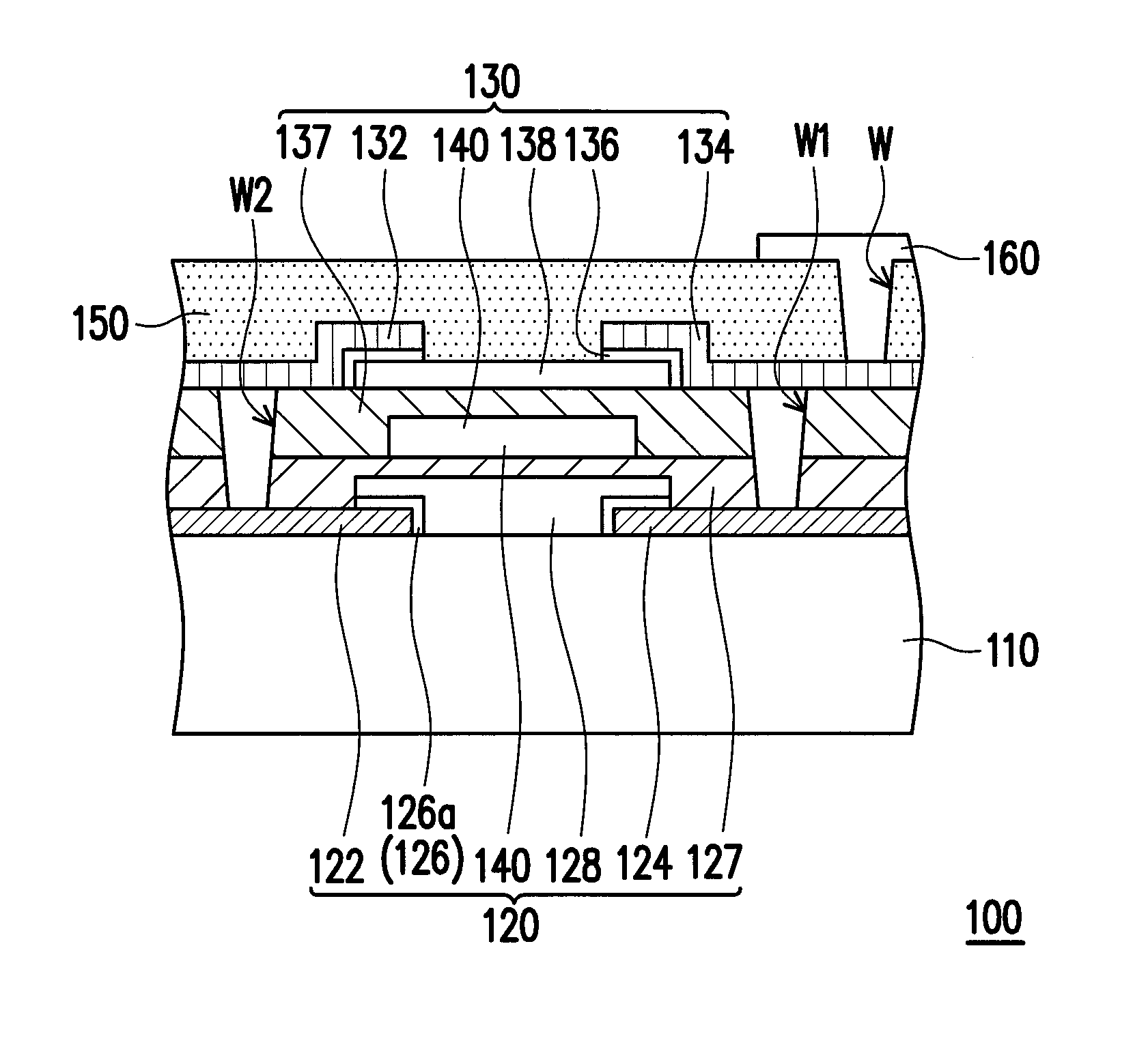
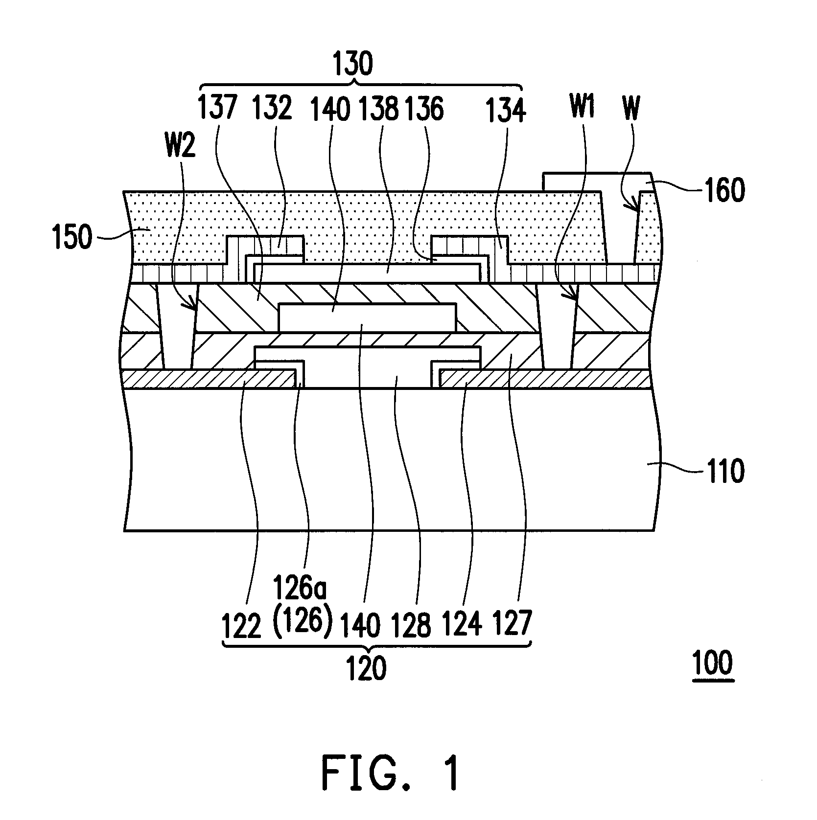
[0031]FIG. 1 is a schematic cross-sectional view of an active device array substrate according to the disclosure. Referring to FIG. 1, an active device array substrate 100 of this embodiment includes a substrate 110, a first transistor 120, a second transistor 130, a common gate electrode 140, a protective layer 150, and a pixel electrode 160. The first transistor 120 is disposed on the substrate 110, wherein the first transistor 120 includes a first channel layer 128. The second transistor 130 is stacked on the first transistor 120, wherein the second transistor 130 includes a second channel layer 138. The first transistor 120 and the second transistor 130 share the common gate electrode 140, and the common gate electrode 140 is disposed between the first channel layer 128 and the second channel layer 138.
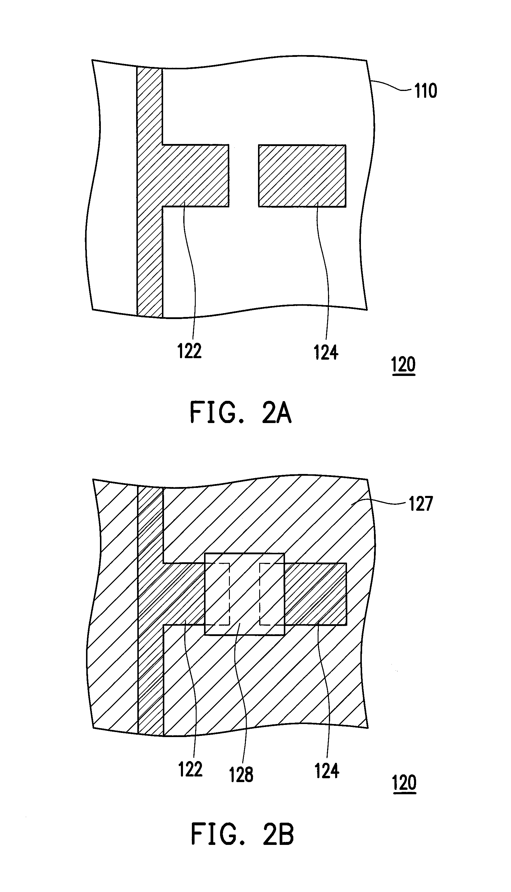
[0032]More specifically, the first transistor 120 includes a first source 122, a first drain 124, a first doped amorphous silicon layer 126, and a first gate insulating layer 127....
third embodiment
[0050]FIG. 6A is a schematic top view of an active device in an active device array substrate according to the disclosure, which is an improvement to the layout space of the active device in the conventional active device array substrate of FIG. 5. FIG. 6B is a schematic cross-sectional view taken along the line A-A′ in FIG. 6A. Referring to FIGS. 6A and 6B, identical elements are indicated by the same reference numbers. According to the disclosure, the first transistor 320 and the second transistor 330 in the active device 300 of FIG. 5 are stacked in the form of a three-dimensional structure, and the first drain 224 of the first transistor 320 and the second drain 134 of the second transistor 330 are electrically connected through the first contact via W1, so as to connect the two transistor 320 and 330 in series. In addition, an opening W is formed in the protective layer 150 on the second drain 134 of the second transistor 330, and the signal outputting trace 380 is electrically...
PUM
 Abstract
Description
Claims
Application Information


