Organic light emitting diode touch display panel

a technology of light-emitting diodes and touch-emitting diodes, which is applied in the direction of discharge tubes luminescnet screens, instrumentation, etc., can solve the problems of limiting the thickness and manufacturing costs and achieve the effect of reducing the thickness of organic light-emitting diodes touch-emitting diodes and saving the material cost of substrates and circuit boards

Active Publication Date: 2014-12-02
HANNSTAR DISPLAY CORPORATION
View PDF0 Cites 2 Cited by
  • Summary
  • Abstract
  • Description
  • Claims
  • Application Information

AI Technical Summary

Benefits of technology

[0007]It is therefore an objective of the present invention to provide an organic light emitting diode touch display panel to reduce the thickness and manufacturing cost.
[0010]The organic light emitting diodes and the touch sensing capacitors are formed on the same substrate in the present invention, instead of extra substrate used to dispose the touch sensing capacitors. The magnetic sensing wire loops is directly disposed on the second substrate in the present invention instead of being disposed on the circuit board. Thus, the thickness of the organic light emitting diode touch display panel can be effectively reduced, and the material cost of the substrate and the circuit board can be saved. Also, the manufacturing step of combining the circuit board and the display panel or the touch panel and the display panel can be ignored.

Problems solved by technology

However, with the progress of the display being developed toward thin thickness and small size, the method of stacking the organic light emitting diode panel and the touch panel to form the organic light emitting diode touch display panel will limit the thickness and the manufacturing cost of the organic light emitting diode touch display panel.

Method used


Image

  • Organic light emitting diode touch display panel
  • Organic light emitting diode touch display panel
  • Organic light emitting diode touch display panel

Examples


Embodiment Construction

[0020]To provide a better understanding of the present invention, exemplary embodiments will be detailed as follows. The exemplary embodiments of the present invention are illustrated in the accompanying drawings with numbered elements to elaborate the contents and effects to be achieved.

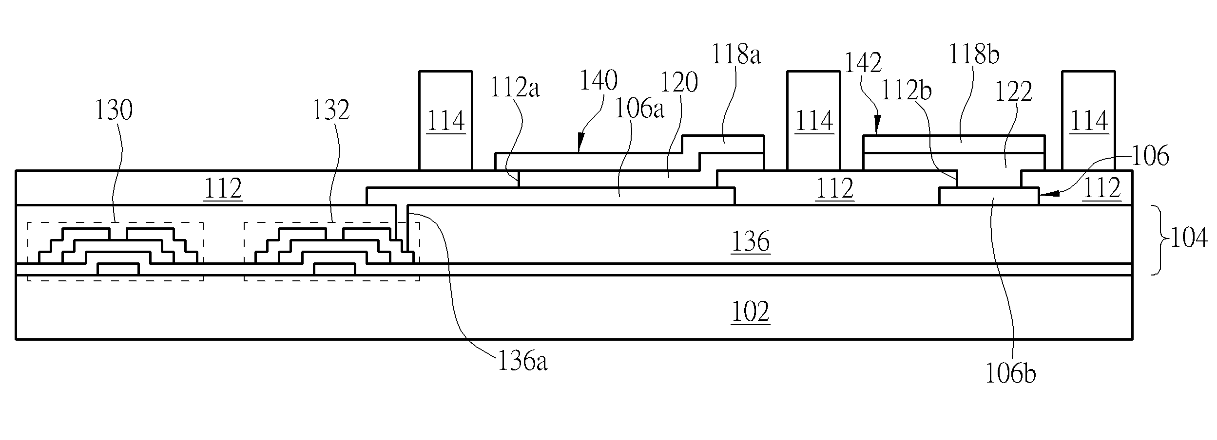
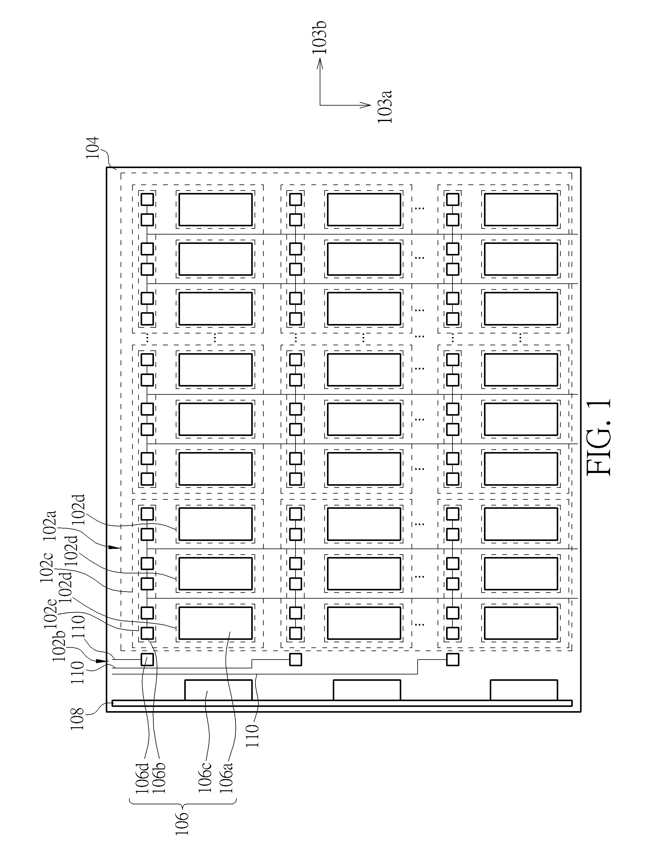
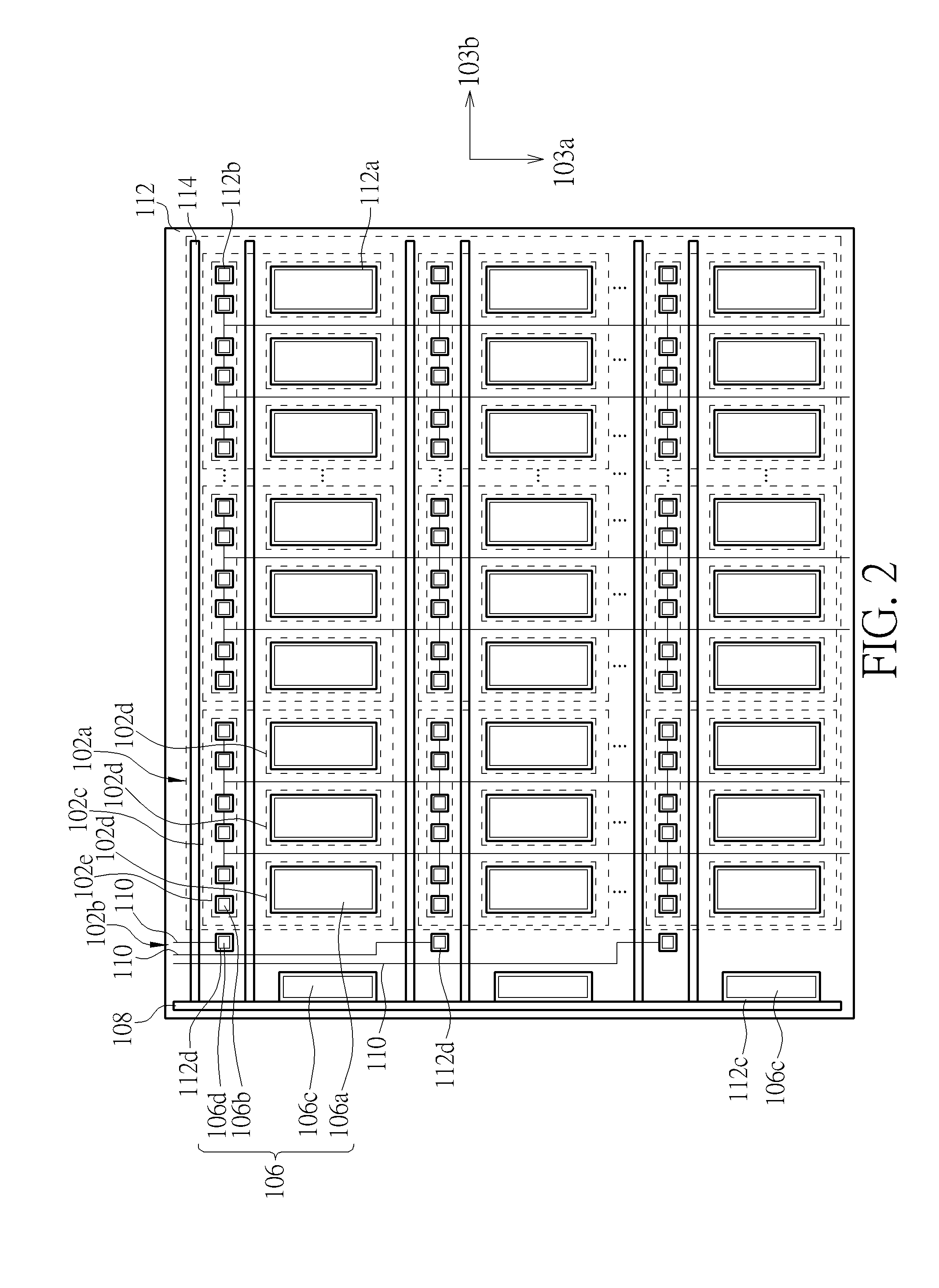
[0021]Please refer to FIG. 1 through FIG. 3. FIG. 1 through FIG. 3 are schematic diagrams illustrating a manufacturing method of an organic light emitting diode touch display panel according to a first embodiment of the present invention, wherein FIG. 3 is a schematic diagram illustrating a top view of the organic light emitting diode touch display panel according to the first embodiment of the present invention. As shown in FIG. 1, a first substrate 102, such as glass substrate, plastic substrate or silicon substrate is provided first. The first substrate 102 has a thin-film transistor layer 104 disposed thereon. Next, a photolithographic process and an etching process are performed to form a first...


PUM


Abstract

The present invention provides an organic light emitting diode touch display panel including a substrate, a plurality of first electrodes and a plurality of second electrodes disposed on the substrate, a plurality of light emitting layers, a plurality of dielectric layers, a plurality of first electrode stripes, and a plurality of second stripes. Each light emitting layer is disposed on each first electrode, and each dielectric layer is disposed on each second electrode. Each first electrode stripe is disposed on the light emitting layers in each row, and each second electrode stripe is disposed on the dielectric layers in each row. Each first electrode, each light emitting layer and each first electrode stripe form an organic light emitting diode, and each second electrode, each dielectric layer and each second electrode stripe form a touch sensing capacitor.

Description

BACKGROUND OF THE INVENTION[0001]1. Field of the Invention[0002]The present invention relates to an organic light emitting diode touch display panel, and more particularly, to an organic light emitting diode touch display panel integrated with a capacitive sensing device.[0003]2. Description of the Prior Art[0004]With technology advanced, the organic light emitting diode display panel has been a newly popular flat display because of having advantages of self light emitting, wide viewing angle, fast response time, high illumination efficiency, low operating voltage, thin panel thickness, available to be formed to be flexible panel, and easy process. Thus, the organic light emitting diode display panel can be applied to various flat display products. In addition, with the touch panel having touching function being developed, more and more application products of the touch display panel formed with the touch panel and display panel are invented, such as mobile phone, GPS navigator syst...

Claims


Application Information

Patent Timeline
Patent Type & Authority Patents(United States)
IPC IPC(8): H01L35/24H01L51/00H01L29/08H01L27/32G06F3/041
CPCG06F3/041H01L27/323G06F3/0412G06F3/0443H10K59/40
Inventor HUANG, CHIEN-HSIANGTSAI, KUN-HUACHUNG, JUN-SHIHCHEN, CHUN-HSI
Owner HANNSTAR DISPLAY CORPORATION
Why Eureka
Try Eureka