Interfacing between an integrated circuit and a waveguide through a cavity located in a soft laminate

a soft laminate and integrated circuit technology, applied in waveguide devices, impedence networks, electrical devices, etc., can solve the problems of radiation loss, skin effect resistance, radiation loss, and the inability to dissipate the signal's power, and achieve the effect of low-loss interfa

Active Publication Date: 2014-12-16
SIKLU COMM
View PDF29 Cites 6 Cited by
  • Summary
  • Abstract
  • Description
  • Claims
  • Application Information

AI Technical Summary

Benefits of technology

[0013]connecting the mm-wave integrated circuit to the surface at the contact location through the connection bumps, such that a first of the connection bumps connects a signal output of the mm-wave integrated circuit to the transmission line, thereby providing the low loss interface.
[0025]a plurality of connection bumps on a surface of the mm-wave integrated circuit providing a connection between the mm-wave integrated circuit and the surface at the contact location, such that a first one of the connection bumps connects a signal output of the mm-wave integrated circuit to the transmission line, thereby providing the low loss interface.

Problems solved by technology

A problem arises as to how to create a low loss interface between a millimeter-wave RFIC and a wave-guide.
The difficulty existing today is that the known interfacing techniques still dissipate the signal's power and are relatively complicated and costly to implement.
Parasitic effects such as skin effect resistance, radiation loss, mutual coupling between bonding wires, and wire inductances are however present, and difficult to control or model.
However the metal leads are of non-uniform width and are closely spaced, leading to electrical characteristics which are difficult to predict or model.
TAB technology is also relatively expensive.

Method used


Image

  • Interfacing between an integrated circuit and a waveguide through a cavity located in a soft laminate
  • Interfacing between an integrated circuit and a waveguide through a cavity located in a soft laminate
  • Interfacing between an integrated circuit and a waveguide through a cavity located in a soft laminate

Examples


Embodiment Construction

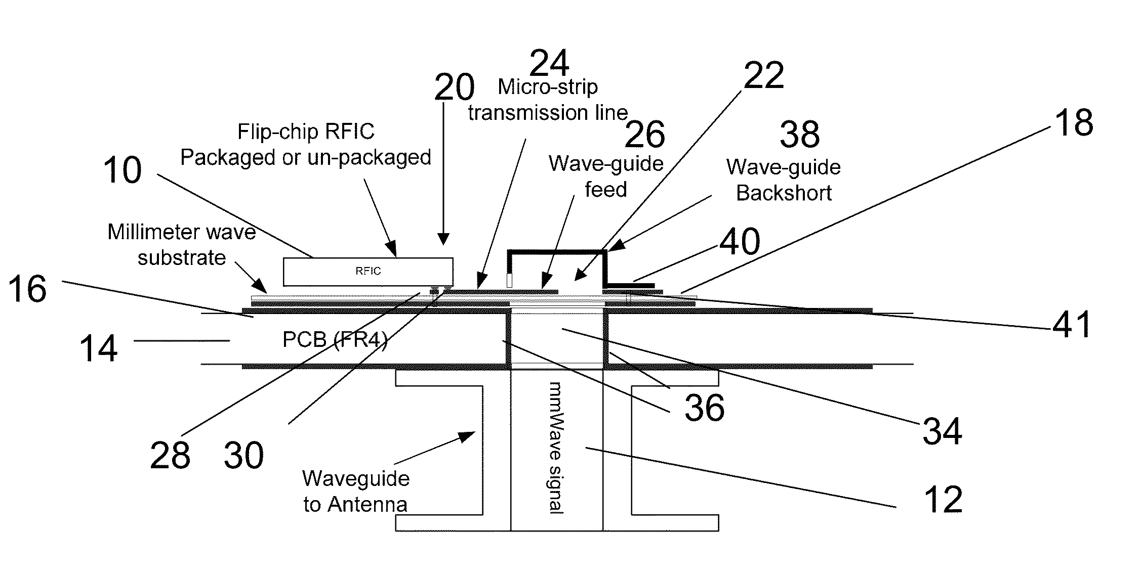
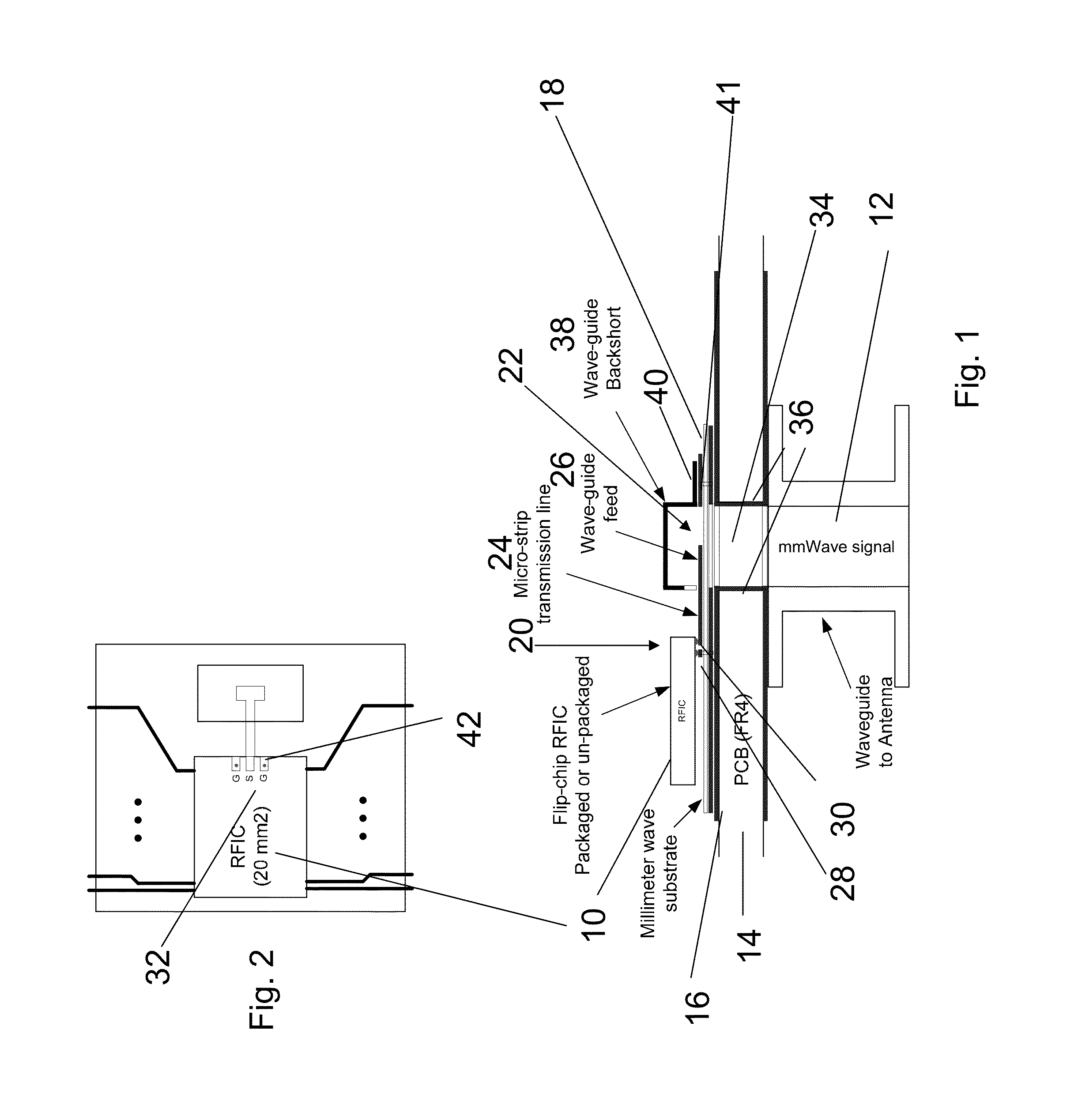
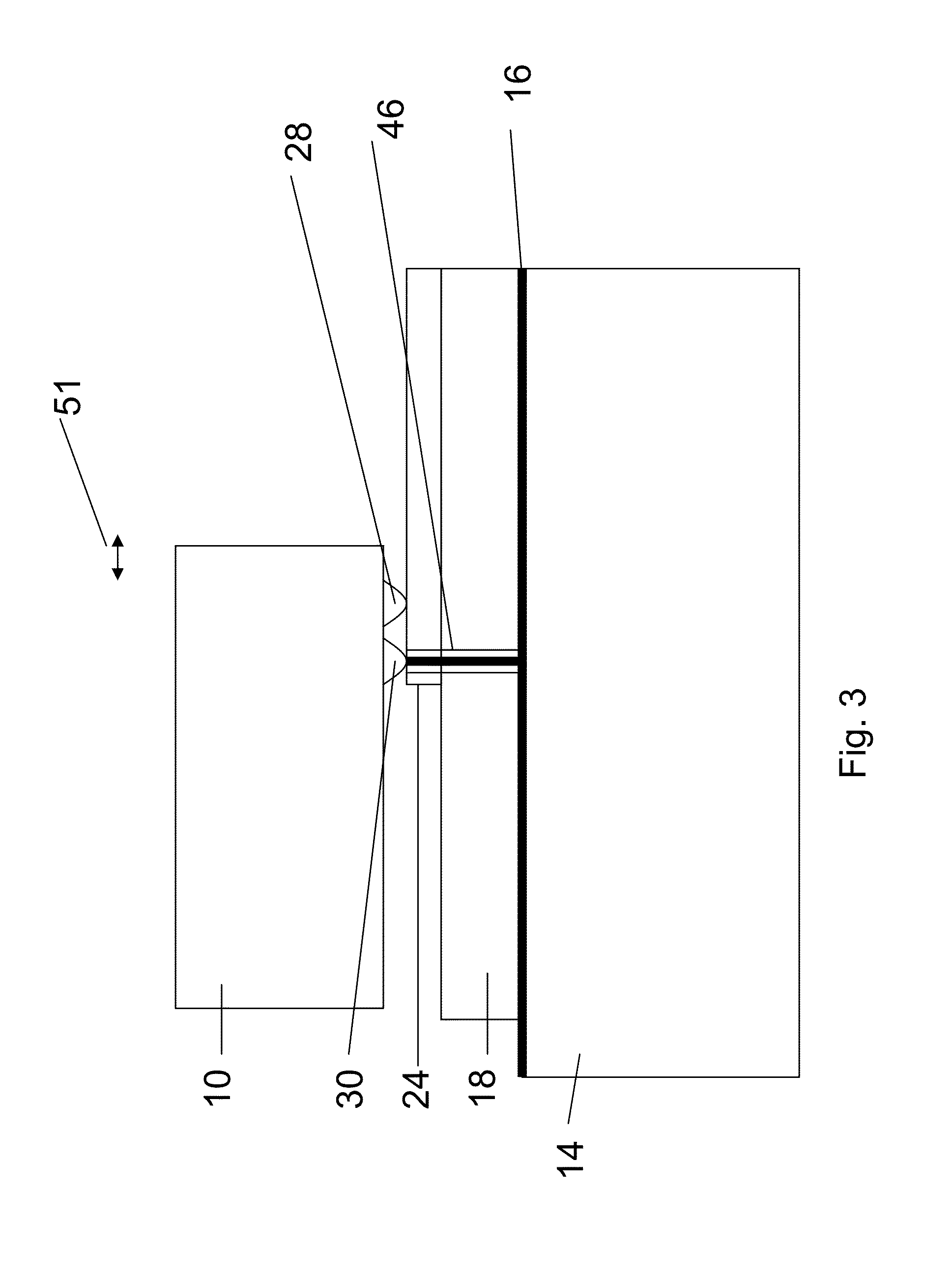
[0047]The present embodiments comprise the use of flip chip style interconnection bumps from an underside ground-signal-ground interface of an RFIC to a microstrip transmission line to link via a waveguide feed to a waveguide, thereby providing an efficient interface between the RFIC and the waveguide. The connection bump is located over the ground-signal-ground signal output of the RFIC and over the microstrip transmission line and forms a connection therebetween. The dielectric overlap between the RFIC and the PCB may be minimized.

[0048]The principles and operation of an apparatus and method according to the present invention may be better understood with reference to the drawings and accompanying description.

[0049]Before explaining at least one embodiment of the invention in detail, it is to be understood that the invention is not limited in its application to the details of construction and the arrangement of the components set forth in the following description or illustrated i...


PUM

PropertyMeasurementUnit
surface areaaaaaaaaaaa
physical lengthaaaaaaaaaa

Abstract

A low-loss interface between a mm-wave integrated circuit and a waveguide comprises a surface having a contact location for said integrated circuit and a waveguide location for fixing a waveguide thereon; a transmission line extending along said surface from said contact location to the waveguide location and extending into the waveguide location as a waveguide feed; and a connection bump on a surface of the mm-wave integrated circuit. The mm-wave integrated circuit RFIC is connected to the surface at the contact location through the connection bump, such as to connect a signal output of the RFIC to the transmission line, thereby providing said low loss interface.

Description

FIELD AND BACKGROUND OF THE INVENTION[0001]The present invention relates to a device and method for interfacing between an integrated circuit and a waveguide and, more particularly, but not exclusively to providing an interface that is efficient at radio and mm-wave frequencies.[0002]A problem arises as to how to create a low loss interface between a millimeter-wave RFIC and a wave-guide.[0003]Current IC production techniques allow a number of types of mechanical structures that can be used to interface IC signals. In order to drive a signal in and out of a wave-guide the mechanical structure needs to comply with specific electromagnetic requirements. In order to drive a millimeter-wave signal between the IC signal interface and the wave-guide's own interface, another mechanical structure is required, the structure having its own electromagnetic requirements in order to drive the electromagnetic signal with minimal loss of signal power.[0004]The difficulty existing today is that the...

Claims


Application Information

Patent Timeline
Patent Type & Authority Patents(United States)
IPC IPC(8): H01P5/107
CPCH01P5/107Y10T29/49016
Inventor DAYAN, ELADSHMUEL, AMIRLEIBA, YIGALSCHWARZ, BARUCH
Owner SIKLU COMM
Why Eureka
Try Eureka