Organic electroluminescence device and electronic apparatus

a technology of electroluminescence device and electronic apparatus, which is applied in the direction of discharge tube luminescnet screen, discharge tube/lamp details, electric discharge lamps, etc., can solve the problem of not being able to perform a display in a desired color, and achieve excellent display quality and less color deviation

Active Publication Date: 2014-12-23
SEIKO EPSON CORP
View PDF56 Cites 10 Cited by
  • Summary
  • Abstract
  • Description
  • Claims
  • Application Information

AI Technical Summary

Benefits of technology

[0011]Therefore, compared to an organic electroluminescence device which does not include a configuration of the application example, it is possible to prevent light, which is shifted to a wavelength longer than the first peak wavelength, which is an intended peak wavelength, and has the second peak wavelength, from being mixed into luminescence from the first luminescence element. Accordingly, it is possible to provide an organic electroluminescence device which has less color deviation and has an excellent display quality.Application Example 2
[0015]In this case, it is possible to adjust a difference between a first peak wavelength of the first light, which is enhanced by the first resonator structure in a portion overlapping the first portion of a functional layer, and the second peak wavelength of the second light, which is enhanced by the first resonator structure in a portion overlapping the second portion of the functional layer, using a film thickness of an insulation layer. Accordingly, it is possible to provide an organic electroluminescence device which can be manufactured in a simpler manufacturing process and has an excellent display quality.Application Example 4
[0018]Therefore, compared to an organic electroluminescence device which does not include a configuration of the application example, it is possible to prevent light having the fourth peak wavelength, which is shifted to a wavelength longer than the third peak wavelength which is an intended peak wavelength, from being mixed into luminescence from a second luminescence element.
[0024]In this case, because of the organic electroluminescence device described in any of the application examples, it is possible to provide an electronic apparatus which has less color deviation and an excellent display quality.

Problems solved by technology

When a color filter transmits light shifted to the long wavelength side and light of the originally intended peak wavelength, even if the color filter is provided with respect to an EL element, there is a problem that light mixture where light of different colors is mixed occurs and makes it impossible to perform a display in a desired color.

Method used


Image

  • Organic electroluminescence device and electronic apparatus
  • Organic electroluminescence device and electronic apparatus
  • Organic electroluminescence device and electronic apparatus

Examples


first embodiment

Organic Electroluminescence Device

[0037]FIG. 1 is a schematic plan view showing a basic configuration of an organic electroluminescence device according to an embodiment 1.

[0038]First, a schematic configuration of an organic electroluminescence (EL) device 100 according to the embodiment 1 will be described.

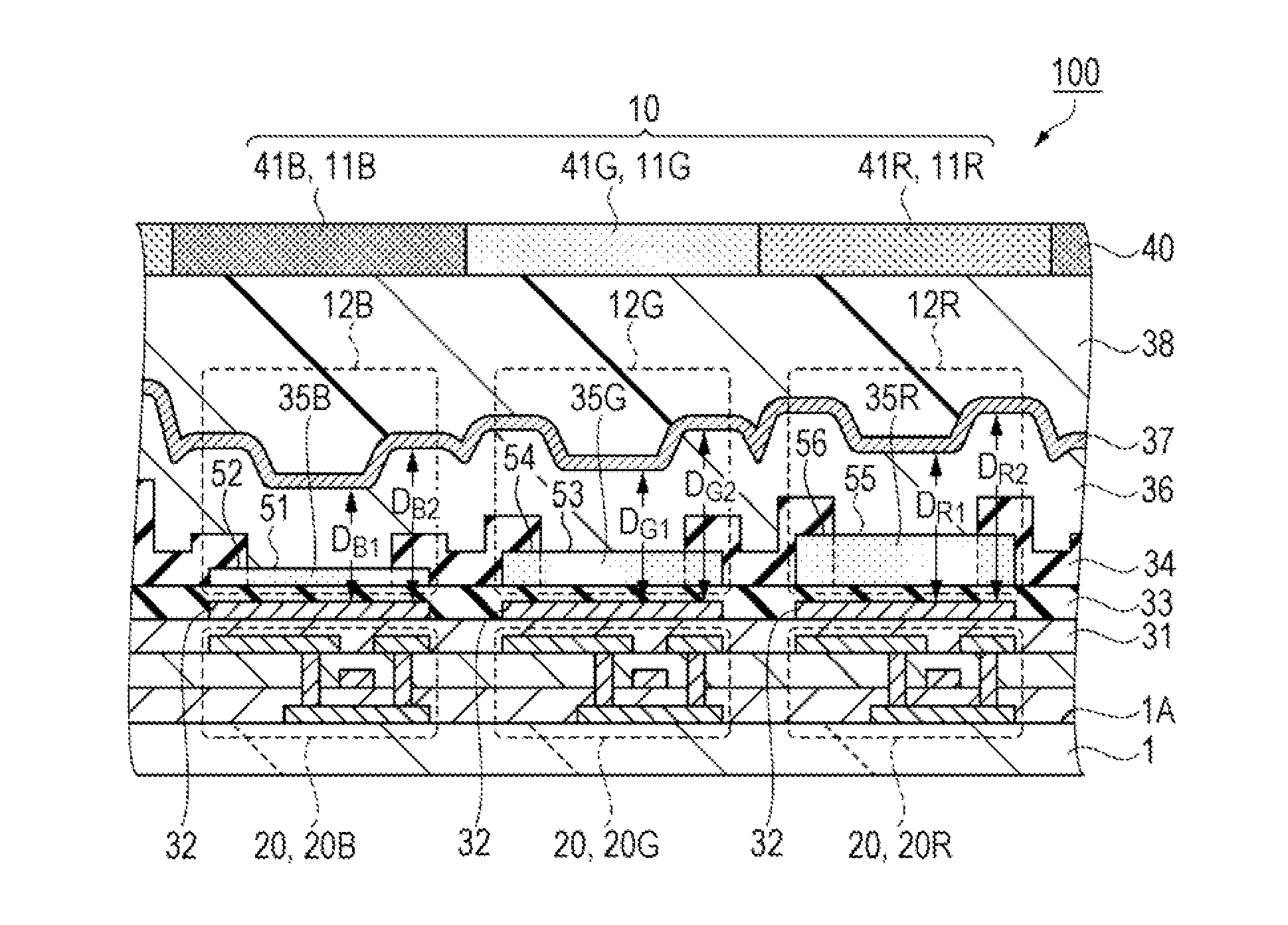
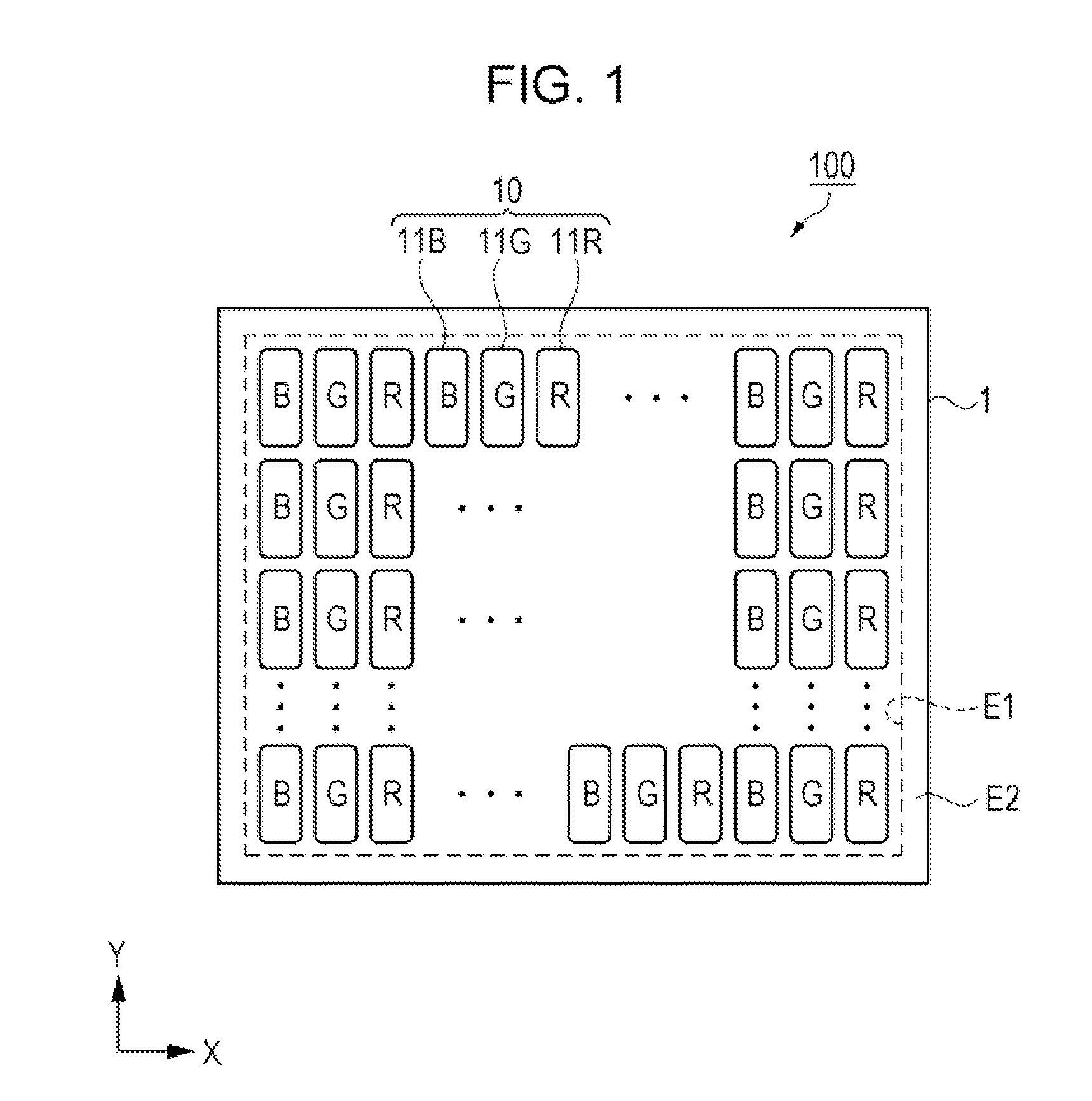
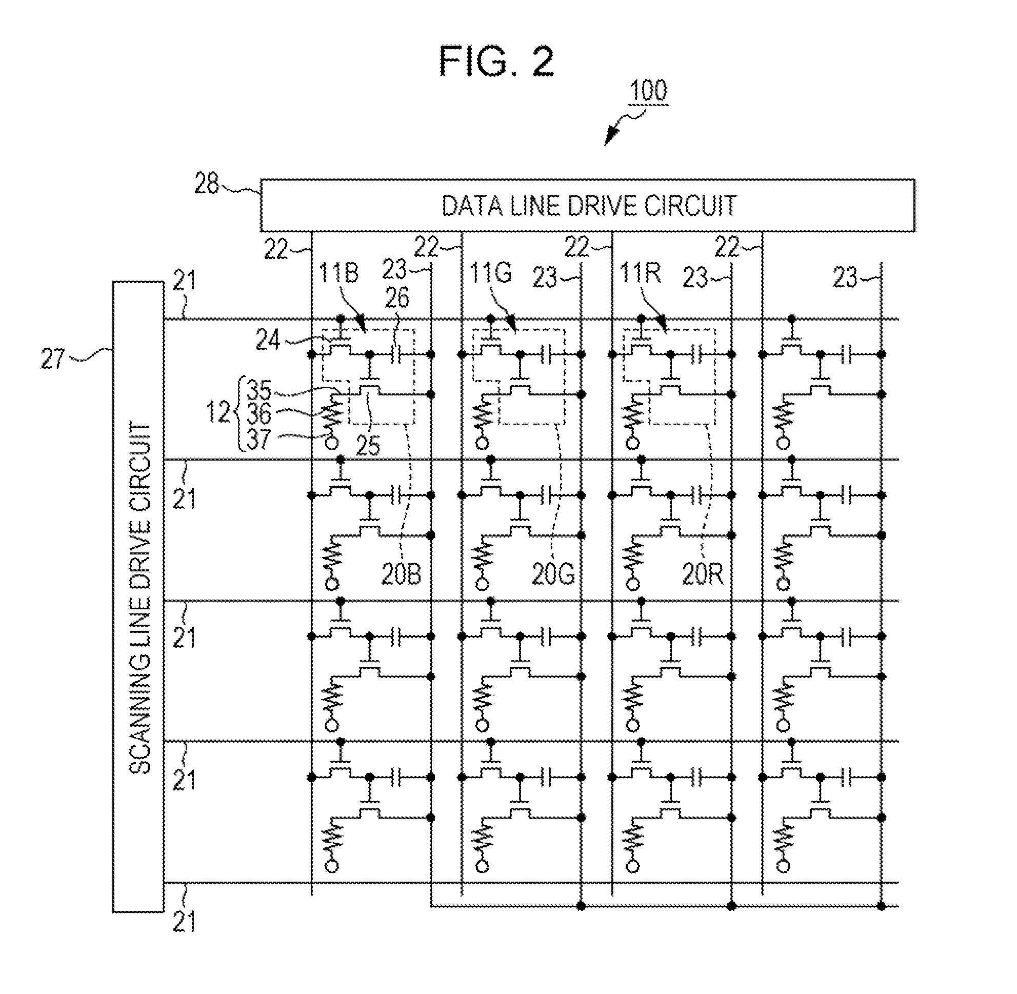
[0039]As shown in FIG. 1, the organic EL device 100 of the embodiment includes a substrate 1, and a plurality of pixels 10 disposed in a display region E1 on a first surface of the substrate 1. In a non-display region E2 between the display region E1 and a peripheral edge of the substrate 1, a peripheral circuit for causing a pixel 10 to emit light is provided. An example of the peripheral circuit includes a scanning line drive circuit, a data line drive circuit, a test circuit, and the like.

[0040]The plurality of pixels 10 is disposed in a matrix shape in the display region E1, and configured to have a plurality of sub-pixels 11 which emit light of different wavelengths, for exa...

first modification example

[0124]In the embodiment 1 described above, film thicknesses of the insulation layer 34 disposed in each of the blue sub-pixel 11B, the green sub-pixel 11G, and the red sub-pixel 11R is the same as each other. However, film thicknesses of the insulation layer 34 disposed in each sub-pixel 11B, 11G, and 11R may be different from each other, film thicknesses of the insulation layer 34 disposed in two sub-pixels among these sub-pixels 11B, 11G, and 11R may be the same as each other, and a film thickness of the insulation layer 34 disposed in the remaining one sub-pixel may be different from film thicknesses of the insulation layer 34 disposed in the other two sub-pixels. Specifically, film thicknesses of the insulation layer 34 disposed in the blue sub-pixel 11B and the green sub-pixel 11G may be the same as each other, and film thicknesses of the insulation layer 34 disposed in the blue sub-pixel 11B and the red sub-pixel 11R may be the same as each other. Film thicknesses of the insul...

second modification example

[0126]In addition, in the embodiment 1 described above, the film thickness of the insulation layer 34 is adjusted in all the sub-pixels 11 of blue (B), green (G), and red (R). However, the insulation layer 34 in one type or two types of sub-pixel 11 may have the film thickness which is not adjusted.

[0127]In general, it is known that a green light is easily visible to human eyes, and it is unlikely to sense the color deviation which occurs even if the abnormal luminescence is mixed in light emitted from the luminescence element 12G. In this case, even if the film thickness of the insulation layer 34 disposed in the green sub-pixel 11G is not adjusted, it is possible to provide the organic EL device 100 which has an excellent display quality.

[0128]Similarly, when the color deviation is unlikely to be visible even if the abnormal luminescence is mixed in light emitted from the blue luminescence element 12B, the film thickness of the insulation layer 34 disposed in the blue sub-pixel 11...


PUM


Abstract

An organic EL device includes a substrate, a first colored layer, a first luminescence element having a first pixel electrode, a reflection layer, and an insulation layer which overlaps a second portion without overlapping a first portion of a first pixel electrode. Light emitted from the first luminescence element includes a first light emitted from a region overlapping a first portion and a second light emitted from a region overlapping a second portion, and a film thickness of an insulation layer or optical characteristics of the first colored layer are set so that the first light is transmitted through the first colored layer more than the second light is.

Description

BACKGROUND[0001]1. Technical Field[0002]The present invention relates to an organic electroluminescence (EL) device and an electronic apparatus including the organic EL device.[0003]2. Related Art[0004]An EL device of active matrix type which includes an EL element interposing an organic electroluminescence layer between a cathode and an anode and a transistor and a capacitor for controlling the drive of the EL element has been known. In the EL device, in order to electrically insulate anodes adjacent to each other, there is provided a passivation layer which has an opening on the anode and where the bottom end of the opening extends on the anode (JP-A-08-241048).[0005]In addition, an organic luminescence element has been known which stacks a semi-transparent reflective layer, a transparent conductive layer, a luminescence layer formed of an organic thin film, and a back electrode on a transparent substrate, and in which an optical resonator is provided between the semi-transparent ...

Claims


Application Information

Patent Timeline
Patent Type & Authority Patents(United States)
IPC IPC(8): H01J63/04H01J1/62H05B33/22
CPCH01L51/5265H01L51/5253H01L27/322H05B33/22H01L27/3244H10K59/38H10K59/12H10K50/844H10K50/852
Inventor IWATA, SHINICHI
Owner SEIKO EPSON CORP
Why Eureka
Try Eureka