Light-emitting device and lighting device

a technology of light-emitting devices and lighting devices, which is applied in the direction of discharge tubes/lamp details, organic semiconductor devices, discharge tubes/lamp details, etc., can solve the problems of high manufacturing yield, small light-emitting region of devices manufactured using metal masks, and difficult to use photolithography techniques utilizing solvents. , to achieve the effect of high reliability, high manufacturing yield and high reliability

Inactive Publication Date: 2015-01-06
SEMICON ENERGY LAB CO LTD
View PDF51 Cites 11 Cited by
  • Summary
  • Abstract
  • Description
  • Claims
  • Application Information

AI Technical Summary

Benefits of technology

[0010]However, a metal mask is much inferior in alignment accuracy and patterning accuracy to a photomask used in a photolithography step. Accordingly, a sufficient space is required around a deposition region in performing selective deposition with the use of a metal mask. In other words, area loss in patterning with the use of a metal mask is much larger than that in patterning in a photolithography step. Therefore, a lighting device manufactured using a metal mask has a small light-emitting region because of the area loss. In order to obtain desired luminance, a lighting device with a small light-emitting region requires larger current than a lighting device with a large light-emitting region. However, degradation is accelerated due to large current, and thus, the lifetime might be adversely affected. Further, the shorter the distance between a metal mask and a substrate is, the more accurately a pattern can be formed; however, a light-emitting layer or the like which has already been formed might be damaged in the case where the metal mask is so close to the substrate as to be in contact with a surface of the substrate. In addition, dust or the like attached to the metal mask might be attached to the substrate in some cases. Damage of a light-emitting layer, attachment of dust, or the like causes defects such as a short circuit and formation of a non-light-emitting region, leading to a decrease in reliability and manufacturing yield.
[0041]The lighting device according to an embodiment of the present invention is a lighting device with high reliability. The lighting device according to an embodiment of the present invention is a lighting device with a high manufacturing yield. The lighting device according to an embodiment of the present invention is a lighting device with high reliability and low power consumption. The lighting device according to an embodiment of the present invention is a lighting device with a high manufacturing yield and low power consumption. The lighting device according to an embodiment of the present invention is a lighting device with high reliability, a high manufacturing yield, and low power consumption.

Problems solved by technology

On the other hand, when patterning is performed on the other electrode, the patterning is performed after a light-emitting layer containing an organic compound is formed; therefore, it is extremely difficult to use a photolithography technique utilizing a solvent.
However, a metal mask is much inferior in alignment accuracy and patterning accuracy to a photomask used in a photolithography step.
Therefore, a lighting device manufactured using a metal mask has a small light-emitting region because of the area loss.
However, degradation is accelerated due to large current, and thus, the lifetime might be adversely affected.
Further, the shorter the distance between a metal mask and a substrate is, the more accurately a pattern can be formed; however, a light-emitting layer or the like which has already been formed might be damaged in the case where the metal mask is so close to the substrate as to be in contact with a surface of the substrate.
In addition, dust or the like attached to the metal mask might be attached to the substrate in some cases.
Damage of a light-emitting layer, attachment of dust, or the like causes defects such as a short circuit and formation of a non-light-emitting region, leading to a decrease in reliability and manufacturing yield.

Method used


Image

  • Light-emitting device and lighting device
  • Light-emitting device and lighting device
  • Light-emitting device and lighting device

Examples


embodiment 1

(Embodiment 1)

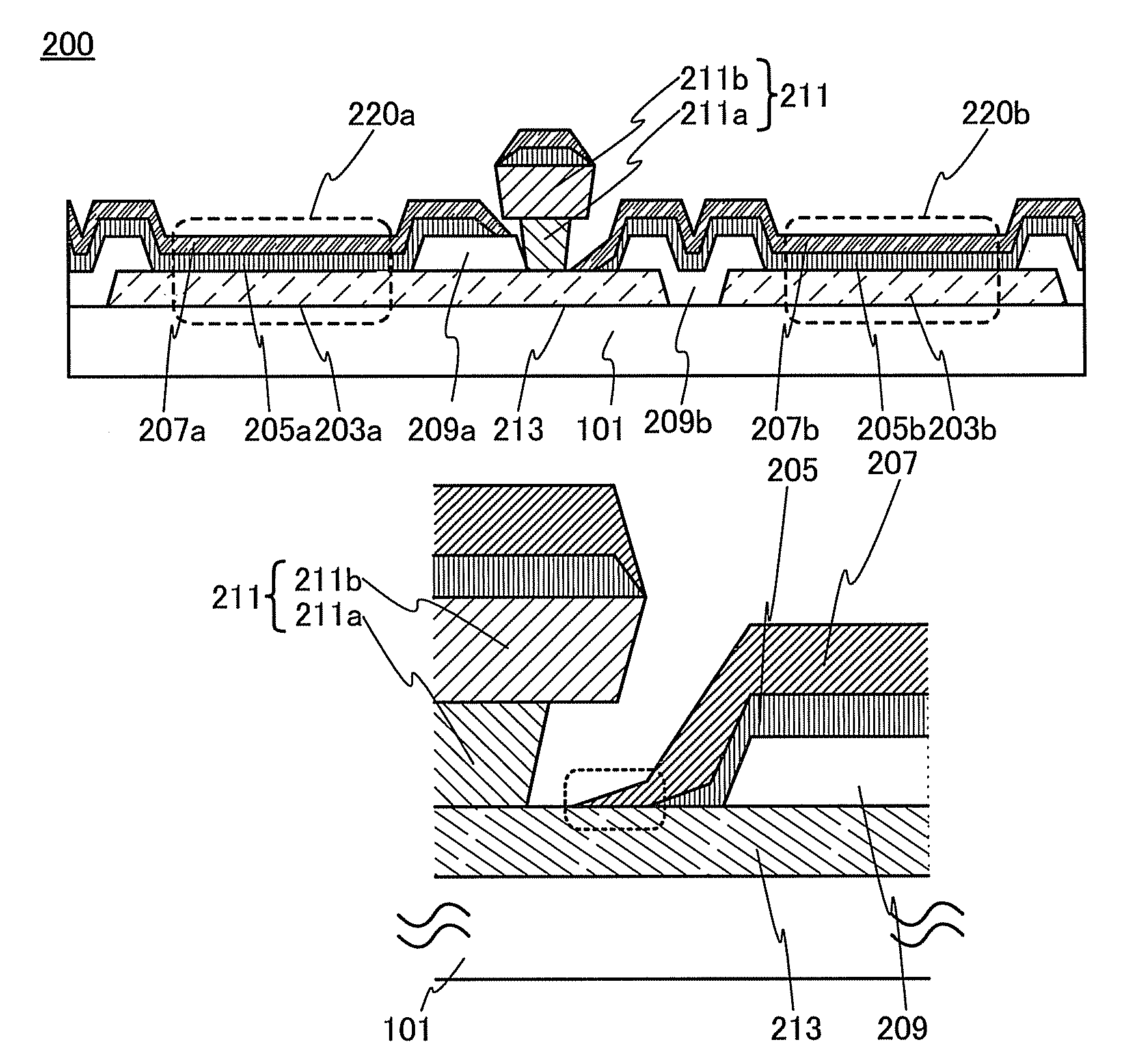
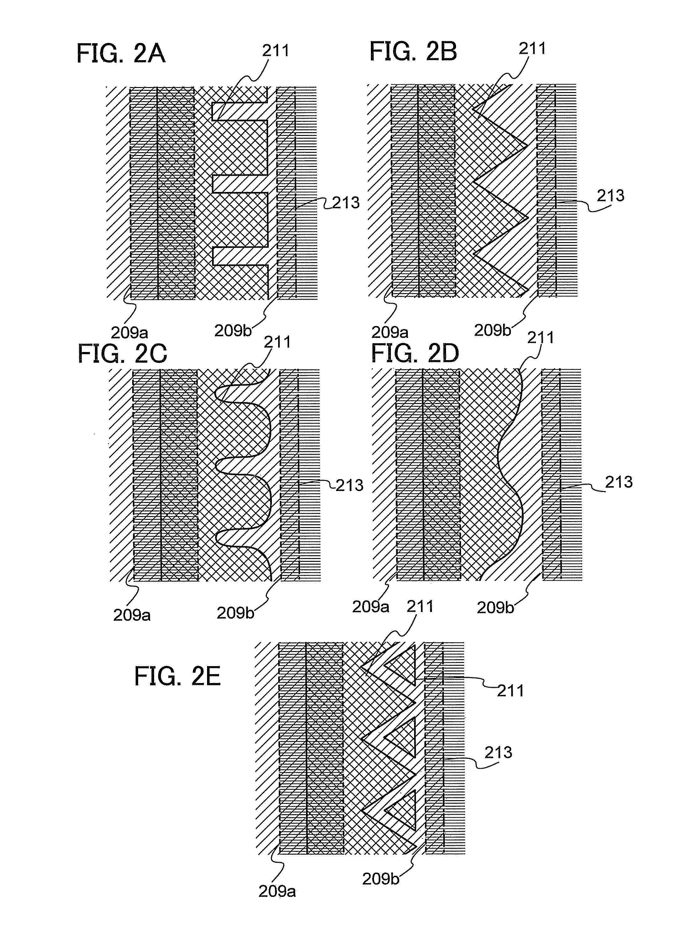
[0058]FIGS. 1A and 1B are schematic cross-sectional views of a light-emitting device according to an embodiment of the present invention. Note that here, part of the light-emitting device according to an embodiment of the present invention is illustrated. FIG. 1A is a schematic cross-sectional view of a light-emitting device 200 including an EL element. In the light-emitting device 200, a first electrode 203, an EL layer 205, and a second electrode 207 are provided in this order over the substrate 101 having an insulating surface, and a portion where these components are in contact with one another is a light-emitting region 220 of the EL element.

[0059]In this specification, it has already been stated that in the case where a plurality of light-emitting regions is provided, the light-emitting regions which include electrodes having the same potential are considered to be in one EL element even in the case where the light-emitting regions are separated. In contrast, whe...

embodiment 2

(Embodiment 2)

[0084]FIG. 4 is a cross-sectional view of a light-emitting device according to an embodiment of the present invention, which is different from that in Embodiment 1. Note that FIG. 4 illustrates part of the light-emitting device according to an embodiment of the present invention. As in the light-emitting device in FIGS. 1A and 1B, in the light-emitting device in FIG. 4, a first electrode 303, an EL layer 305, and a second electrode 307 are provided in this order over the substrate 101 having an insulating surface, and a portion where these components are in contact with one another is a light-emitting region 320 of an EL element. In the EL element, an electrode layer on the side from which light is extracted is formed using a material which transmits light from the EL layer. For example, a light-transmitting conductive material is used for the second electrode 307 in the case of a top-emission type, for the first electrode 303 in the case of a bottom-emission type, or ...

embodiment 3

(Embodiment 3)

[0102]FIG. 6 is a schematic top view of a light-emitting device 300 according to an embodiment of the present invention, in which the structure in Embodiment 1 and the structure in Embodiment 2 are combined.

[0103]The light-emitting device 300 includes four EL elements (a first EL element a, a second EL element b, a third EL element c, and a fourth EL element d) surrounded by the separation layer 311. The four EL elements are connected in series by a series connection portion 350a, a series connection portion 350b, a series connection portion 350c, and a series connection portion 350d. Since the structure of the series connection portions is described in Embodiment 1, the description is omitted here. The description in Embodiment 1 is to be referred to. A cross-sectional view taken along line A-A′ in FIG. 6 corresponds to the cross-sectional view in FIG. 1A described in Embodiment 1.

[0104]Note that the EL layer 305, the second electrode 307, and the like are not illustr...


PUM


Abstract

A highly reliable light-emitting device or lighting device is provided. Further, a light-emitting device or lighting device with a high manufacturing yield is provided. Provided is a light-emitting device having a contact structure which includes a separation layer having a shape typified by a reverse tapered shape in which an outline of the bottom portion is inside an outline of an upper portion and which utilizes the difference between an amount of a light-emitting layer extending inside the outline and that of an upper electrode extending inside the outline. Further, when the outline of the separation layer which forms the contact portion has a depression and a projection, the length of the contact portion can be increased, and thus, contact resistance can be reduced.

Description

BACKGROUND OF THE INVENTION[0001]1. Field of the Invention[0002]The present invention relates to a light-emitting device or a lighting device including an EL element in which a light-emitting layer containing an organic compound is interposed between a pair of electrodes.[0003]2. Description of the Related Art[0004]In recent years, a light-emitting element (also referred to as an electroluminescent (EL) element) in which a light-emitting layer (hereinafter also referred to as an EL layer) containing an organic compound is interposed between a pair of electrodes has been actively developed. Lighting has attracted attention as one of application fields of the light-emitting element. This is because a lighting device including the EL element has features different from those of other lighting devices; for example, the lighting device including the EL element can be thin and light, and perform surface emission.[0005]In addition, an EL element has attracted attention also in terms of its...

Claims


Application Information

Patent Timeline
Patent Type & Authority Patents(United States)
IPC IPC(8): H01L29/18H01L27/32H01L51/52
CPCH01L27/3204H01L51/5212H01L51/5228H01L2251/5361H10K59/86H10K50/814H10K50/824H10K50/805H10K50/85
Inventor TANADA, YOSHIFUMIMORI, HIDENORI
Owner SEMICON ENERGY LAB CO LTD
Why Eureka
Try Eureka