Semiconductor memory device including memory cells and a peripheral circuit and method of operating the same

a memory device and semiconductor technology, applied in the field can solve the problems of deteriorating operational characteristics and reduced cell current of semiconductor memory devices, and achieve the effect of improving operational characteristics

Active Publication Date: 2015-01-20
SK HYNIX INC +1
View PDF15 Cites 10 Cited by
  • Summary
  • Abstract
  • Description
  • Claims
  • Application Information

AI Technical Summary

Benefits of technology

[0005]Embodiments of the present invention are directed to a semiconductor memory device having enhanced operational characteristics and a method of operating the same.
[0006]In accordance with an embodiment of the present invention, a semiconductor memory device includes a memory block configured to include memory strings coupled to and disposed between bit lines and a common source line; and a peripheral circuit configured to perform a read operation of memory cells included in selected memory strings of the memory strings, and increase channel potential of memory strings not selected in the read operation.
[0008]A semiconductor memory device of the present invention may have enhanced operational characteristics.

Problems solved by technology

As a result, cell current reduces and operational characteristics of the semiconductor memory device deteriorate.

Method used


Image

  • Semiconductor memory device including memory cells and a peripheral circuit and method of operating the same
  • Semiconductor memory device including memory cells and a peripheral circuit and method of operating the same
  • Semiconductor memory device including memory cells and a peripheral circuit and method of operating the same

Examples


first embodiment

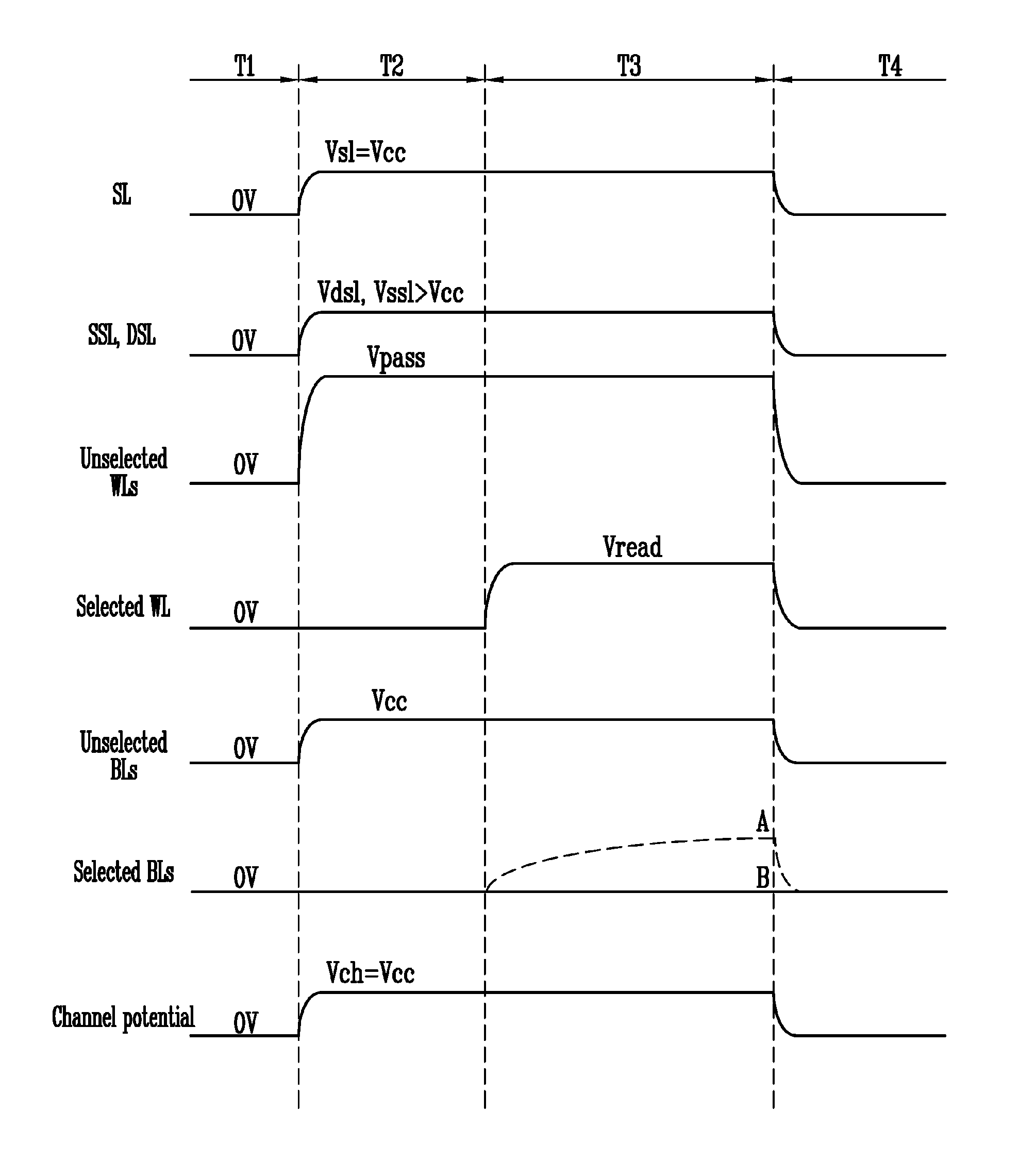
[0069]As shown in FIG. 10, a difference between current that flows from a common source line SL to a selected bit line through a channel area of a selected memory string when every unselected memory cell is in an erase state Al and current when every unselected memory cell is in a program state B1 is great when the read operation in the first embodiment is performed on a first memory cell coupled to a source select transistor in the selected memory string.

second embodiment

[0070]Further, a difference between current when every unselected memory cell is in an erase state A2 and current when every unselected memory cell is in a program state B2, is also great when the read operation in the second embodiment shown in FIG. 4 is performed on the first memory cell coupled to the source select transistor in the selected memory string, but an amount of the current flowing from the common source line SL to the selected bit line through the channel area of the selected memory string increases. As a result, a change of the threshold voltage according to the state of the unselected memory cells is reduced compared to with a conventional technique.

third embodiment

[0071]Referring to FIG. 10, a difference between current when every unselected memory cell is in an erase state A3 and current when every unselected memory cell is in a program state B3, substantially reduces when the read operation in accordance with the third embodiment shown in FIG. 5 is performed on the first memory cell coupled to the source select transistor in the selected memory string. Accordingly, change of the threshold voltage according to the state of the unselected memory cells is considerably reduced compared to with the conventional technique.

[0072]In the event that the above read operation is performed, current flowing in the selected memory string increases, change of the threshold voltage due to the read disturb may be minimized even though the number of the read operations performed increases, and the deterioration of operational characteristics due to back pattern dependency may be reduced as shown in FIG. 10. As a result, operational characteristics and reliabi...


PUM


Abstract

A semiconductor memory device includes a memory block including memory strings coupled to and disposed between bit lines and a common source line, and a peripheral circuit configured to perform a read operation of memory cells included in selected memory strings of the memory strings and increase channel potential of unselected memory strings in the read operation.

Description

CROSS-REFERENCE TO RELATED APPLICATION[0001]This application claims priority from Korean Patent Application No. 10-2012-0009076, filed on Jan. 30, 2012, the contents of which are incorporated herein by reference in their entirety.BACKGROUND[0002]Embodiments of the present invention relate to a semiconductor memory device including a plurality of memory cells and a method of operating the same.[0003]As the degree of integration of a semiconductor memory device increases, memory cell size decreases and space between memory cells narrows. As a result, cell current reduces and operational characteristics of the semiconductor memory device deteriorate.[0004]Accordingly, a method of enhancing the operational characteristics of the semiconductor memory device has been required.SUMMARY OF THE INVENTION[0005]Embodiments of the present invention are directed to a semiconductor memory device having enhanced operational characteristics and a method of operating the same.[0006]In accordance with...

Claims


Application Information

Patent Timeline
Patent Type & Authority Patents(United States)
IPC IPC(8): G11C16/26G11C16/02G11C16/04
CPCG11C16/02G11C16/26G11C16/0483G11C7/10G11C16/06G11C16/24
Inventor LEE, JONG, HO
Owner SK HYNIX INC
Why Eureka
Try Eureka