
Systems and methods for fabrication of superconducting integrated circuits

a technology of integrated circuits and fabrication methods, applied in the direction of superconductor devices, instruments, dissimilar materials junction devices, etc., can solve the problems of gold contaminating a fabrication tool, contaminating the semiconductor facilities, and not using quantum gates and circuits

Active Publication Date: 2015-02-10
D WAVE SYSTEMS INC
View PDF18 Cites 32 Cited by
  • Summary
  • Abstract
  • Description
  • Claims
  • Application Information

AI Technical Summary

Problems solved by technology

This approach may not make use of quantum gates and circuits.
This may be due to the fact that some of the materials used in superconducting integrated circuits can contaminate the semiconductor facilities.
For instance, gold may be used as a resistor in superconducting circuits, but gold can contaminate a fabrication tool used to produce CMOS wafers in a semiconductor facility.
Consequently, superconducting integrated circuits containing gold are not processed by tools which also process CMOS wafers.
Due to issues unique to superconducting circuits, not all semiconductor processes and techniques are necessarily transferrable to superconductor chip manufacture.
Such changes and adjustments typically are not obvious and may require a great deal of experimentation.
The semiconductor industry faces problems and issues not necessarily related to the superconducting industry.
Likewise, problems and issues that concern the superconducting industry are often of little or no concern in standard semiconductor fabrication.
Therefore, if a Josephson junction is deposited on the substrate of a superconducting integrated circuit, any dielectric layers, such as silicon dioxide, subsequently deposited within the circuit cannot be done at the semiconductor industry standard temperature of around 400 degrees Celsius.
Low temperature deposition of silicon dioxide can result in a large number of defects within the dielectric.
Such defects can be seen as noise during the operation of superconducting integrated circuits.
Any impurities within superconducting chips may result in noise which can compromise or degrade the functionality of the individual devices, such as superconducting qubits, and of the superconducting chip as a whole.
Also, niobium, a material chosen more for its high superconducting critical temperature than its suitability to fabrication, does not naturally fill via holes very well.
This can result in poor contacts between wiring layers of superconducting integrated circuits.
Plugs have been thought of as a way to avoid the problems of filling high aspect ratio holes with niobium, but unfortunately utilizing plug technology may result in contamination of semiconductor facilities with niobium.
Further, magnetic noise is typically a major concern in the production of superconducting qubits, but may be of little or no concern for many semiconductor chip applications

Method used


Image

  • Systems and methods for fabrication of superconducting integrated circuits
  • Systems and methods for fabrication of superconducting integrated circuits
  • Systems and methods for fabrication of superconducting integrated circuits

Examples


Embodiment Construction

[0050]In the following description, certain specific details are set forth in order to provide a thorough understanding of various disclosed embodiments. However, one skilled in the relevant art will recognize that embodiments may be practiced without one or more of these specific details, or with other methods, components, materials, etc. In other instances, well-known structures associated with superconductive circuits or structures, quantum computer circuits or structures and / or cooling systems such as evaporative refrigerators have not been shown or described in detail to avoid unnecessarily obscuring descriptions of the embodiments.

[0051]Unless the context requires otherwise, throughout the specification and claims which follow, the word “comprise” and variations thereof, such as, “comprises” and “comprising” are to be construed in an open, inclusive sense, that is as “including, but not limited to.”

[0052]Reference throughout this specification to “one embodiment” or “an embodi...


PUM

PropertyMeasurementUnit
temperatureaaaaaaaaaa
widthaaaaaaaaaa
widthaaaaaaaaaa

Abstract

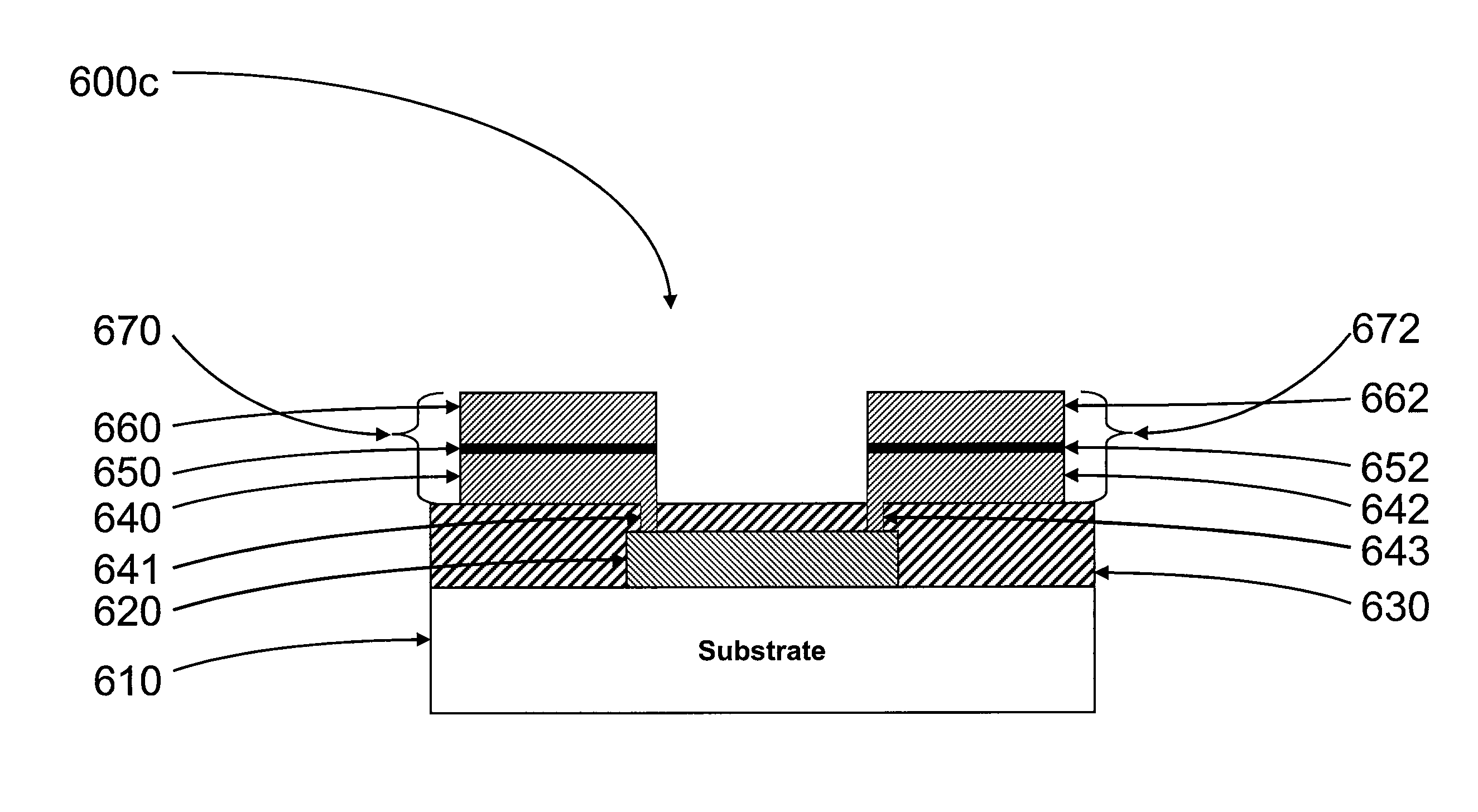
Various techniques and apparatus permit fabrication of superconductive circuits and structures, for instance Josephson junctions, which may, for example be useful in quantum computers. For instance, a low magnetic flux noise trilayer structure may be fabricated having a dielectric structure or layer interposed between two elements or layers capable of superconducting. A superconducting via may directly overlie a Josephson junction. A structure, for instance a Josephson junction, may be carried on a planarized dielectric layer. A fin may be employed to remove heat from the structure. A via capable of superconducting may have a width that is less than about 1 micrometer. The structure may be coupled to a resistor, for example by vias and / or a strap contact connector.

Description

CROSS REFERENCE TO RELATED APPLICATIONS[0001]This application is a U.S. national stage application filed under 35 U.S.C. 371 of International Patent Application PCT / US2010 / 025403, accorded an international filing date of Feb. 25, 2010 which claims benefit under 35 U.S.C. 119(e) of U.S. Provisional Patent Application Ser. No. 61 / 156,377, filed Feb. 27, 2009 and entitled “Systems and Methods for Fabrication of Superconducting Integrated Circuits,” both of which are incorporated herein by reference in its their entirety.BACKGROUNDField[0002]The present systems and methods relate to the fabrication of integrated circuits for superconducting applications.Approaches to Quantum Computation[0003]There are several general approaches to the design and operation of quantum computers. One such approach is the “circuit model” of quantum computation. In this approach, qubits are acted upon by sequences of logical gates that are the compiled representation of an algorithm. Much research has been f...

Claims


Application Information

Patent Timeline
Patent Type & Authority Patents(United States)
IPC IPC(8): H01L29/72B82Y10/00G06N99/00H01L27/18H01L39/22H01L39/24
CPCH01L27/18B82Y10/00G06N99/002H01L39/223H01L39/2493G06N10/00H10N69/00H10N60/12H10N60/0912H01L28/24Y10S977/707Y10S977/723Y10S977/943H10N60/0156H10N60/805
Inventor LADIZINSKY, ERICROSE, GEORDIEHILTON, JEREMY P.DANTSKER, EUGENEOH, BYONG HYOP
Owner D WAVE SYSTEMS INC
Learn More