Supercharge Your Innovation With Domain-Expert AI Agents!

Programmable logic device and method for driving programmable logic device

a logic device and programmable logic technology, applied in the field of programmable logic devices, can solve the problems of increasing power consumption of memory elements including drams or srams, and achieve the effect of high-reliability programmabl

Inactive Publication Date: 2015-02-10
SEMICON ENERGY LAB CO LTD
View PDF131 Cites 10 Cited by
  • Summary
  • Abstract
  • Description
  • Claims
  • Application Information

AI Technical Summary

Benefits of technology

This approach enables reliable configuration and reconfiguration of PLDs across various power supply voltage states, reducing power consumption and improving reliability by managing transitions effectively.

Problems solved by technology

A memory element including a DRAM or an SRAM has a problem of an increase in power consumption due to an increase in leakage current between power supply lines coupled with development of microfabrication technique.

Method used


Image

  • Programmable logic device and method for driving programmable logic device
  • Programmable logic device and method for driving programmable logic device
  • Programmable logic device and method for driving programmable logic device

Examples


embodiment 1

[0046]This embodiment is described with reference to drawings in the following order:

1. Block Diagram of PLD

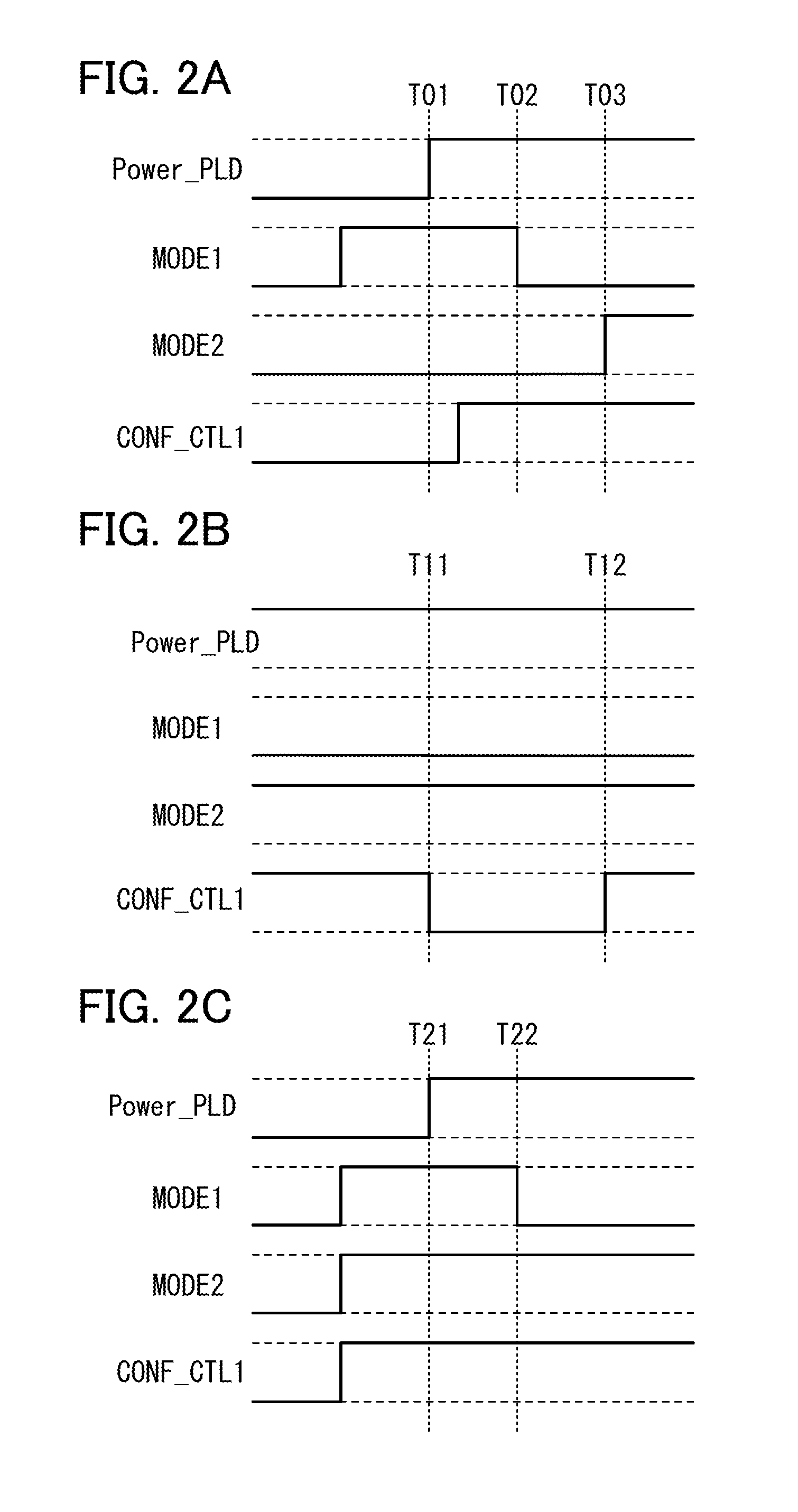
2. Method for Driving PLD

3. Modification of Method for Driving PLD

4. Details of Components in PLD

[0047]4-1. Structure of Logic Array

[0048]4-2. Structure of Switch Portion

[0049]4-3. Structure of LE

[0050]4-4. Structure of Configuration Memory

[0051]4-5. Features of Oxide Semiconductor Transistor

5. Action and Effect of Method for Driving PLD Disclosed in This Specification.

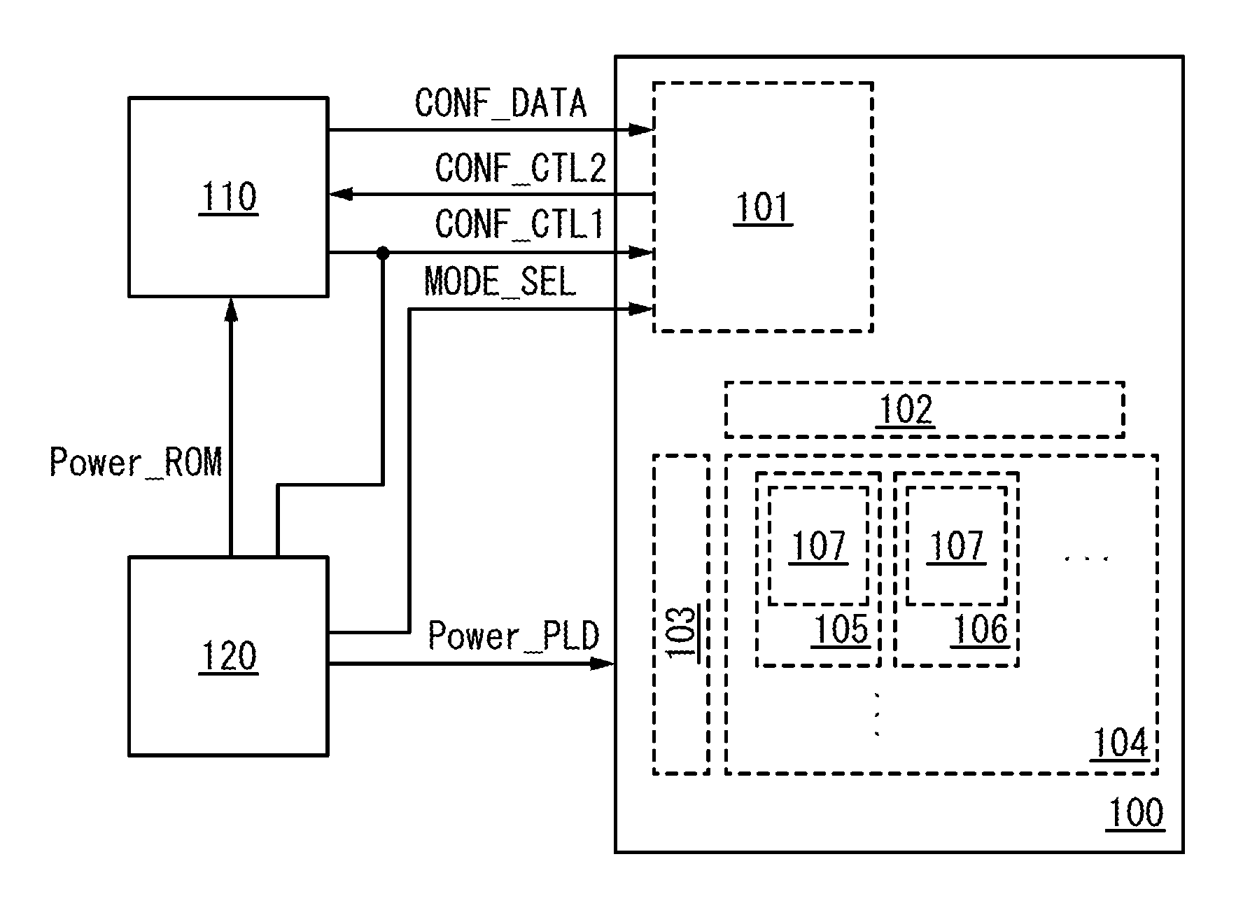
[0052]First, a block diagram of a PLD is described.

[0053]A block diagram in FIG. 1 illustrates a PLD operated by a method for driving a PLD according to one embodiment of the present invention. FIG. 1 illustrates a PLD 100, a storage circuit 110, and a power supply control circuit 120.

[0054]The PLD 100 includes a PLD control circuit 101, a data line driver circuit 102, a word line driver circuit 103, and a logic array 104.

[0055]The logic array 104 includes an LE 105 and a switch portion 106. The LE 105 and the s...

embodiment 2

[0176]A PLD according to one embodiment of the present invention can be used for display devices, personal computers, or image reproducing devices provided with recording media (typically, devices that reproduce the content of recording media such as digital versatile discs (DVDs) and have displays for displaying the reproduced images). Further, as electronic devices that can include the PLD according to one embodiment of the present invention, cellular phones, game machines (including portable game machines), portable information terminals, e-book readers, cameras such as video cameras and digital still cameras, goggle-type displays (head mounted displays), navigation systems, audio reproducing devices (e.g., car audio systems and digital audio players), copiers, facsimiles, printers, multifunction printers, automated teller machines (ATMs), vending machines, and the like can be given. FIGS. 10A to 10F illustrate specific examples of these electronic devices.

[0177]FIG. 10A illustra...


PUM


Abstract

Configuration is performed in accordance with a plurality of states when power supply voltage is supplied intermittently. At the time of start of supply of power supply voltage with configuration, a programmable logic device is sequentially changed into a first state where configuration data is not set in a configuration memory, a second state where the configuration memory is initialized, and a third state where the configuration data can be set in the configuration memory. At the time of start of supply of power supply voltage without configuration, the programmable logic device is sequentially changed into a fourth state where the configuration data is not set in the configuration memory and the third state. The first to fourth states are switched to any one of the states by control of a first state signal and a second state signal.

Description

BACKGROUND OF THE INVENTION[0001]1. Field of the Invention[0002]The present invention relates to semiconductor devices. In particular, the present invention relates to methods for driving programmable logic devices.[0003]Unlike a normal integrated circuit in which all the circuits are fixed at the time of manufacture, a programmable logic device (PLD) can function with an intended circuit structure set by a user at the time of actual use after shipment. Examples of such user-programmable devices are small-scale logics such as a programmable array logic (PAL) and a generic array logic (GAL) and large-scale logics such as a complex programmable logic device (CPLD) and a field programmable gate array (FPGA). In this specification, such devices are called PLDs.[0004]2. Description of the Related Art[0005]PLDs show flexibility in a reduction in development period and a change in design specification compared to conventional application specific integrated circuits (ASICs) and gate arrays...

Claims


Application Information

Patent Timeline
Patent Type & Authority Patents(United States)
IPC IPC(8): G06F7/38H03K19/173H03K19/00H03K19/177
CPCH03K19/17772H03K19/1776H03K19/17748H03K19/0008
Inventor IKEDA, TAKAYUKIKUROKAWA, YOSHIYUKI
Owner SEMICON ENERGY LAB CO LTD
Features
  • R&D
  • Intellectual Property
  • Life Sciences
  • Materials
  • Tech Scout
  • Unparalleled Data Quality
  • Higher Quality Content
  • 60% Fewer Hallucinations
Learn More