Waveguide assembly for a microwave receiver with electro-optic modulator

a microwave receiver and microwave receiver technology, applied in waveguides, waveguide horns, waveguide type devices, etc., can solve the problems of antenna and modulator damage, approach to bandwidth, etc., to prevent electric field breakdown in the waveguide assembly, reduce the effect of incoming electric field concentration, and high dielectric strength

Inactive Publication Date: 2015-03-31
HRL LAB
View PDF56 Cites 23 Cited by
  • Summary
  • Abstract
  • Description
  • Claims
  • Application Information

AI Technical Summary

Benefits of technology

[0013]The metallic tapper preferably has a tapered height and preferably provides an impedance-matching transition between a input end of the waveguide end and a distal end where the electro-optic modulator is preferably located, thereby efficiently concentrating an incoming electric field at the electro-optic modulator. The electro-optic modulato

Problems solved by technology

1. An article by R. C. J. Hsu, A. Ayazi, B. Houshmand, and B. Jalali, entitled “All-dielectric photonic-assisted radio front-end technology”, Nature Photonics, vol. 1, September 2007, pp. The disclosed apparatus uses an electro-optic modulator to sense the level of the microwave signal coupled into a dielectric resonator antenna. The electro-optic modulator is part of an RF-photonic link that provides electrical isolation between the antenna and the rest of the microwave receiver front-end (which contains the sensitive radio components), thereby achieving tolerance to unwanted high power electromagnetic radiation. This prior approach is based on an electro-optic microdisk resonator (acting as the modulator) that is intimately in contact with the dielectric resonator antenna. Because of its resonant antenna, this prior art apparatus couples in substantial power from incident radiation at only those frequencies that match the resonant frequencies of the antenna. Nevertheless, despite its all dielectric construction, the

Method used


Image

  • Waveguide assembly for a microwave receiver with electro-optic modulator
  • Waveguide assembly for a microwave receiver with electro-optic modulator
  • Waveguide assembly for a microwave receiver with electro-optic modulator

Examples


Embodiment Construction

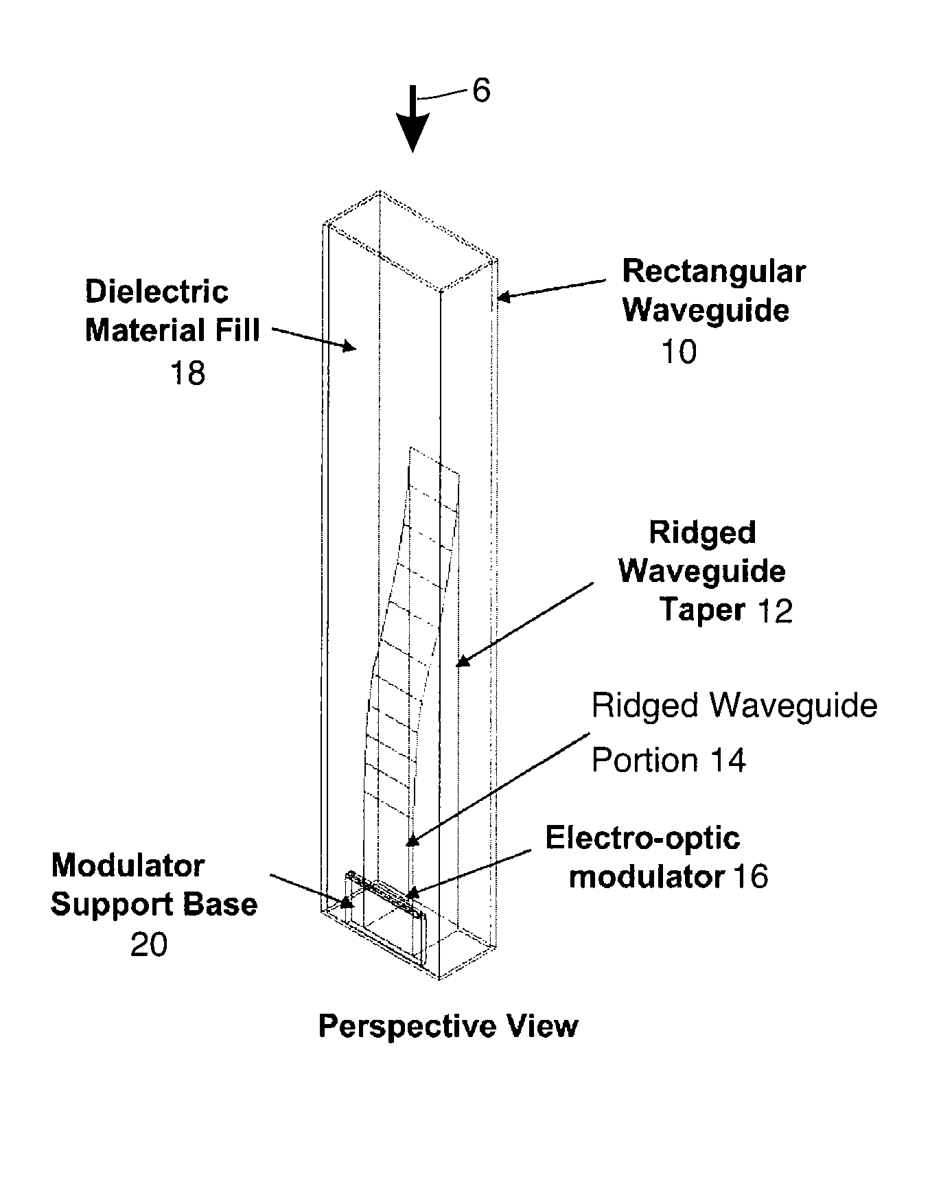
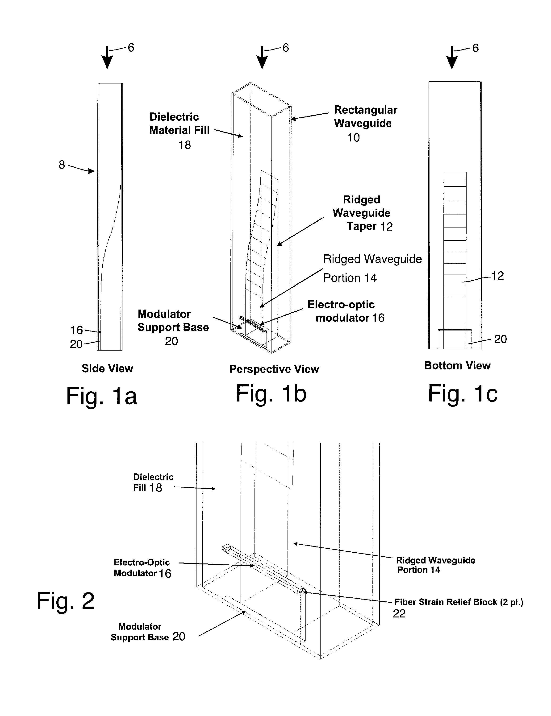
[0031]A basic embodiment of a rectangular waveguide to ridged waveguide assembly is shown in FIGS. 1a-1c. In this embodiment an incident RF signal 6 arrives at a modulator 16 via the rectangular waveguide 10. The waveguide dimensions are selected such that only the TE10 mode propagates. Preferably, the dimensions of the rectangular waveguide 10 are compatible with standard dimension waveguides, such as those designated by the EIA (Electronic Industry Alliance). The TE10 mode is transformed to a single ridged waveguide mode through a ridged waveguide taper 12. The shape of the ridged waveguide taper 12 along the waveguide 10 is determined by the required impedance transformation between the rectangular waveguide 10 and the ridged waveguide 14. Although the impedance of a rectangular waveguide 10 is arbitrary, there is a convention that fixes the impedance based upon the power that flows across the waveguide cross section, and the positive current that flows across the cross-section Z...


PUM


Abstract

A waveguide assembly for a use with, for example, a microwave receiver. The waveguide assembly includes: a waveguide; a tapered structure disposed within the waveguide, the tapered structure tapering in thickness from a first end with a zero height to a second end where the tapered structure has a height which nearly fills, but does not completely fill, the waveguide, to thereby define a modulator receiving space between the tapered structure and an adjacent wall of said waveguide. The second end of the tapered structure is preferably disposed adjacent an open circuited end of the waveguide. An electro-optic modulator is disposed on a dielectric substrate, the dielectric substrate being disposed at least partially within the modulator receiving space and the electro-optic modulator being disposed so that it is located, in use, at an antinode of a standing wave of the waveguide assembly.

Description

CROSS REFERENCE TO RELATED APPLICATIONS[0001]This application is a continuation in part of U.S. Ser. No. 12 / 176,114 filed on Jul. 18, 2008 and entitled “An RF Receiver Front-End Assembly”, and is also related to the following US patent applications: U.S. Ser. No. 12 / 141,825, filed on Jun. 18, 2008 and entitled “Optoelectronic modulator and electric-field sensor with multiple optical-waveguide gratings”; U.S. Ser. No. 12 / 141,834, filed on Jun. 18, 2008 and entitled “Enhanced Linearity RF Photonic Link”; U.S. Ser. No. 12 / 176,089, filed on Jul. 18, 2008 and entitled “Parallel Modulator Photonic Link”; and U.S. Ser. No. 12 / 176,071, filed on Jul. 18, 2008 and entitled “Microwave receiver front-end assembly and array”. The disclosure of each of these related applications is hereby incorporated herein by reference.STATEMENT REGARDING FEDERAL FUNDING[0002]This invention was made under U.S. Government contract W911QX-08-C-0074. The U.S. Government has certain rights in this invention.TECHNIC...

Claims


Application Information

Patent Timeline
IPC IPC(8): H04B10/2575H01P3/16
CPCH01P3/16H01Q13/02H04B10/90H04B2210/006H01P5/087H01P5/107
Inventor SCHAFFNER, JAMES H.GEARY, KEVINYAP, DANIEL
Owner HRL LAB
Why Eureka
Try Eureka