
Magnet assisted alignment method for wafer bonding and wafer level chip scale packaging

a technology of chip scale and wafer, which is applied in the direction of electrical equipment, semiconductor devices, semiconductor/solid-state device details, etc., to achieve the effect of facilitating self-alignment, minimizing the overall magnetic energy of the pairing magnet, and high outpu

Inactive Publication Date: 2015-04-21
GE YI +3
View PDF5 Cites 1 Cited by
  • Summary
  • Abstract
  • Description
  • Claims
  • Application Information

AI Technical Summary

Benefits of technology

The invention proposes a general alignment scheme that can achieve sub-micron accuracy with high output for wafer-to-wafer and chip-to-wafer bonding. It uses specially designed pairing patterned magnets made at the wafer level process, which can be manipulated during bonding to activate or tune the magnetic force between the magnets on the two wafers or chips. This magnetization manipulation assists in the alignment process, which can be achieved by external magnetic field. The force between pairing magnets helps bring the two components close to each other for self-alignment and minimize the overall magnetic energy of the pairing magnets. In chip-to-wafer bonding, all the chips can be placed on the wafer with loose alignment accuracy, and the force between magnets will push for high precision alignment via self-alignment process. This alignment method with high precision alignment can be done for all the chips simultaneously, reducing the bonding time. The patent proposes various patterned magnet structures and materials for the invention, which are based on the magnet pairing principle. The alignment accuracy depends on the size of the patterned magnet pair, photolithography alignment accuracy, and process accuracy. The invention provides a general alignment method that can be extended into a wider implementation.

Problems solved by technology

Precision alignment accuracy in a sub-micron scale, together with high unit-per-hour (UPH), has always been a huge challenge in the electronics and semiconductor industry in the past a few decades.

Method used


Image

  • Magnet assisted alignment method for wafer bonding and wafer level chip scale packaging
  • Magnet assisted alignment method for wafer bonding and wafer level chip scale packaging
  • Magnet assisted alignment method for wafer bonding and wafer level chip scale packaging

Examples


Embodiment Construction

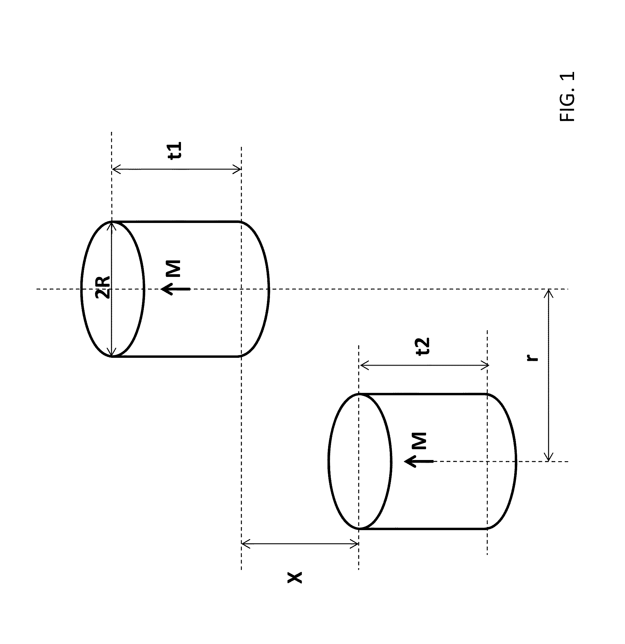
[0021]The present invention relates to the alignment scheme and maintains the alignment during wafer-to-wafer and chip-to-wafer bonding. In order to take the advantage of self-alignment and attractive force between the magnetic north pole (N-pole) and south pole (S-pole), specially designed magnets, which can be brought together for pairing (or matching), are fabricated via wafer level processes. The magnetic force will bring the magnet pair together and align them automatically to minimize the system energy. Using this approach, the alignment accuracy can be greatly improved well beyond the current capability and its ultimate limits lay on the wafer level process capability.

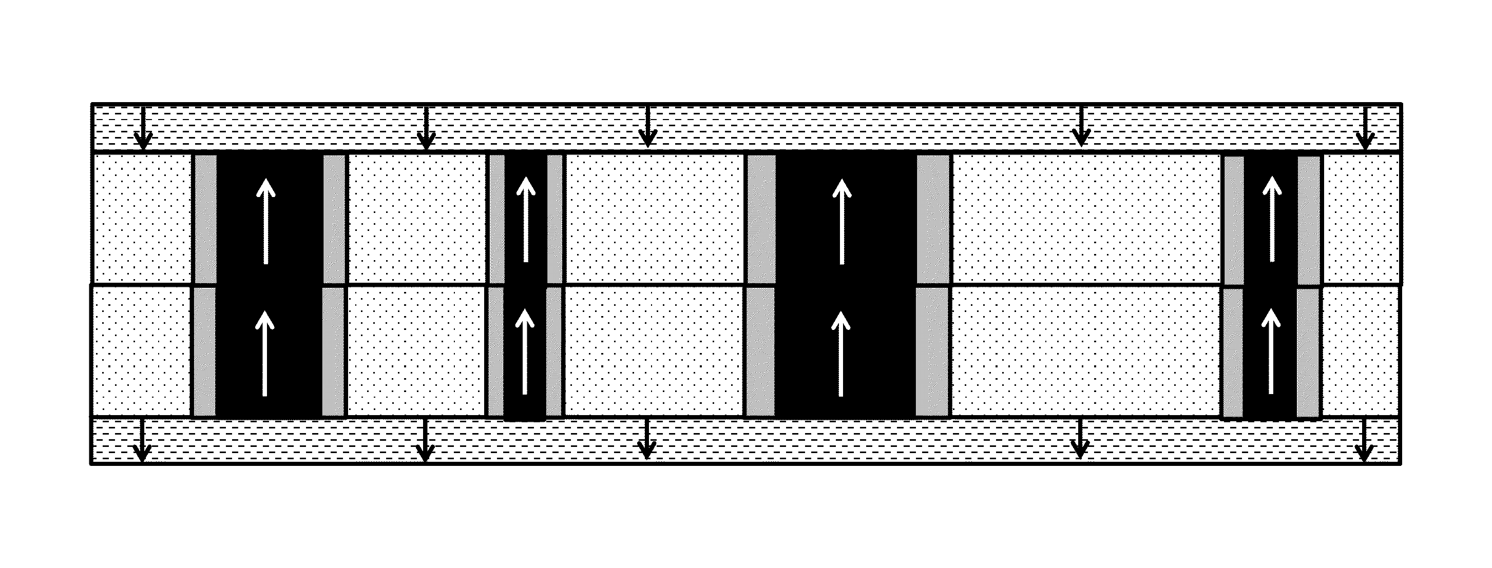
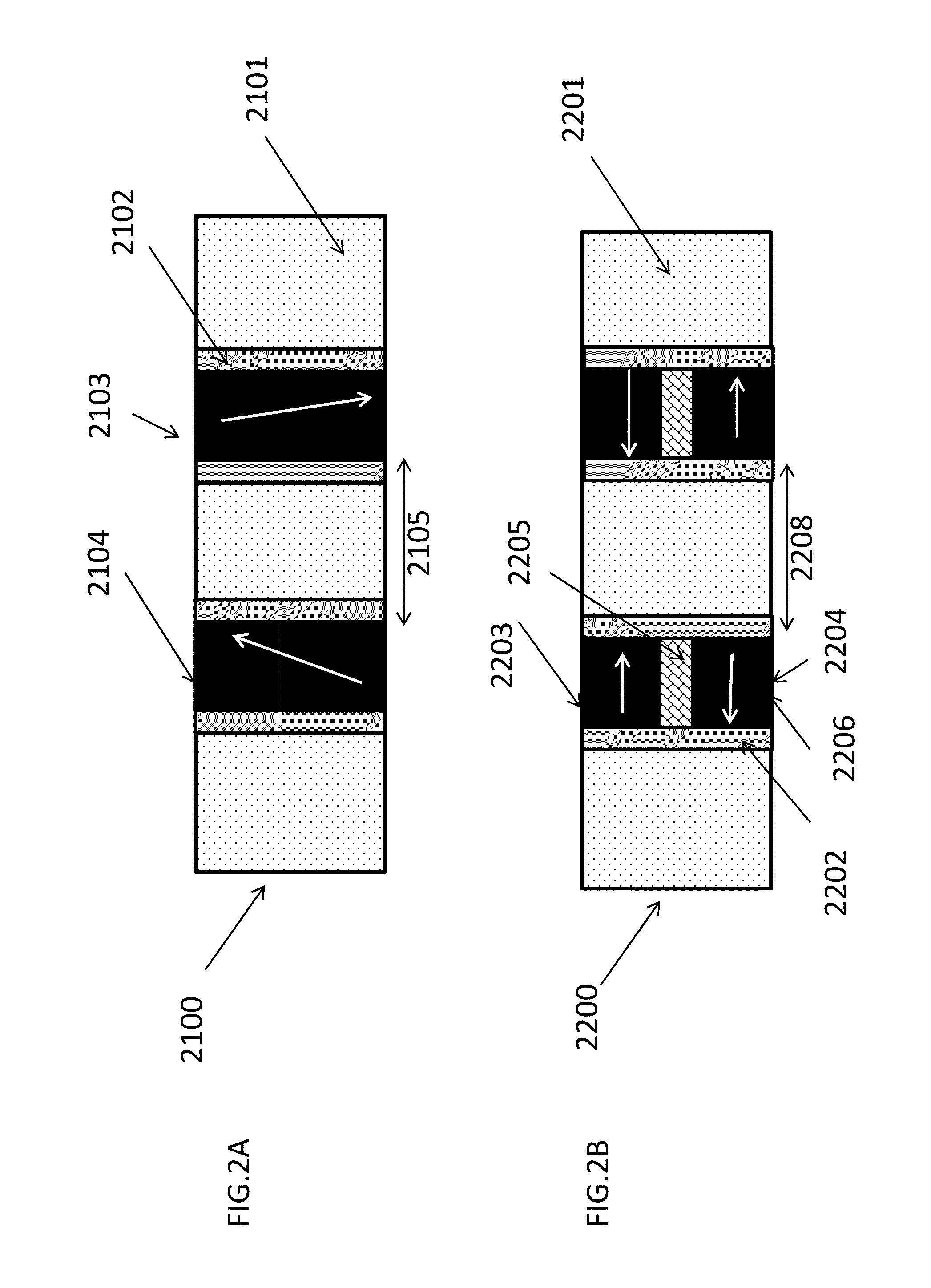
[0022]In details, four kinds of the structures of patterned magnets have been proposed, namely, patterned continue magnetic layer; patterned magnetic sandwich or multilayer; electrical via with built-in magnets; and patterned soft magnets over perpendicular hard magnetic layer. For each kind of the patterned mag...


PUM


Abstract

A high-precision alignment method with high throughput is proposed, which can be used for wafer-to-wafer, chip-to-wafer or chip-to-chip bonding. The scheme implements pairing patterned magnets predetermined designed and made using wafer level process on two components (wafer or chip). The magnetization in patterned magnet can be set at predetermined configuration before bonding starts. When, the two components are bought to close proximity after a coarse alignment, the magnetic force will bring the magnet pairs together and aligned the patterned magnet on one component with its mirrored or complimentary patterned magnets on the other component to minimize the overall the magnetic energy of the pairing magnet. A few patterned magnet structures and materials, with their unique merits are proposed as examples for magnet pair for the self-alignment purpose. This method enables solid contact at the bonding interface via patterned magnets under the magnetic force, which avoid the wafer drafting due to the formation of the liquid phases.

Description

REFERENCE CITED-US PATENT DOCUMENTSFIELD OF INVENTION[0001]The invention is related to precision alignment methodology for wafer-to-wafer bonding or chip-to-wafer bonding, more specifically the utilization of predetermined patterned magnet pairs to facilitate precision wafer-to-wafer or chip-to-wafer alignment for bonding. In order to take the advantage of self-alignment and attractive force between the north pole (N-pole) and south pole (S-pole), specially designed magnets, which can be brought for pairing (or matching), are fabricated via wafer level processes, respectively, on individual bonding wafer or chip. Once the magnetization of the magnets is aligned, while the two wafers or chip are brought to close proximity, the force between the pairing magnets will automatically align the wafers or chip-to-wafer in order to minimize the overall magnetic energy. Specially designed magnets can enable the external field activation or deactivation of the magnet pairing and control the fo...

Claims


Application Information

Patent Timeline
Patent Type & Authority Patents(United States)
IPC IPC(8): H01L21/68H01L23/00
CPCH01L24/83H01L24/80H01L24/81H01L24/94H01L24/97H01L2924/01322H01L2224/05547H01L2224/03614H01L2224/03826H01L2224/80801H01L24/03H01L24/05H01L24/08H01L24/11H01L24/13H01L24/16H01L2224/0345H01L2224/03452H01L2224/03462H01L2224/0362H01L2224/05009H01L2224/05073H01L2224/05082H01L2224/05083H01L2224/05084H01L2224/05124H01L2224/05144H01L2224/05147H01L2224/05155H01L2224/05157H01L2224/05578H01L2224/056H01L2224/05624H01L2224/05644H01L2224/05647H01L2224/05655H01L2224/05657H01L2224/08146H01L2224/1145H01L2224/11452H01L2224/11462H01L2224/1162H01L2224/13022H01L2224/13025H01L2224/131H01L2224/16146H01L2224/80121H01L2224/80143H01L2224/81121H01L2224/81143H01L2224/81801H01L2224/94H01L2224/97H01L2224/05576H01L2224/03612H01L2224/03827H01L2224/80169H01L2224/81169H01L2924/1461H01L2924/00015H01L2924/00014H01L2924/014H01L2924/01026H01L2924/01028H01L2924/01078H01L2924/01024H01L2224/80H01L2224/81H01L2224/03H01L2224/11H01L2924/00H01L2224/0401
Inventor YI, GELIU, ZONGRONGTANG, YUNJUNLI, SHAOPING
Owner GE YI
Learn More