Multi-beam system for high throughput EBI

a multi-beam system and high-throughput technology, applied in the direction of magnetic discharge control, instruments, heat measurement, etc., can solve the problems of increasing the importance of electron beam inspection, long scanning time required to scan the entire surface of the wafer, and the difficulty of using a single-beam scanning electron microscope (sem) for wafer inspection

Active Publication Date: 2015-05-19
ICT INTEGRATED CIRCUIT TESTING GESELLSCHAFT FUER HALBLEITERPRUEFTECHNIK GMBH
View PDF22 Cites 71 Cited by
  • Summary
  • Abstract
  • Description
  • Claims
  • Application Information

AI Technical Summary

Benefits of technology

[0011]According to one embodiment, a scanning charged particle beam device configured to image a specimen is provided. The scanning charged particle beam device includes a source of charged particles, a condenser lens for influencing the charged particles, an aperture plate having at least two aperture openings to generate at least two primary beamlets of charged particles, at least two deflectors configured to individually deflect the at least two primary beamlets of charged particles so that each primary beamlet appears to come from a different source, wherein the at least two deflectors are multi-pole deflectors with an order of poles of 8 or higher, a multi-pole deflector with an order of poles of 8 or higher, an objective lens configured to focus the at least two primary beamlets onto the specimen, wherein the objective lens is a retarding field compound lens, a beam separator configured to separate the at least two primary beamlets from at least two signal beamlets, a beam bender, or a deflector or a mirror configured to deflect the at least two signal beamlets, wherein the beam bender is selected from the group consisting of: a hemispherical beam bender and a beam bender having at least two curved electrodes, and at least two detector elements configured to individually measure the at least two signal beamlets.
[0012]According to another embodiment, an arrayed scanning charged particle beam device is provided. The device includes at least two scanning charged particle beam devices, for example at least 5 scanning charged particle beam devices, or even at least 10 scanning charged particle beam devices. Each of the scanning charged particle beam devices includes a source of charged particles, a condenser lens for influencing the charged particles, an aperture plate having at least two aperture openings to generate at least two primary beamlets of charged particles, at least two deflectors configured to individually deflect the at least two primary beamlets of charged particles so that each primary beamlet appears to come from a different source, wherein the at least two deflectors are multi-pole deflectors with an order of poles of 8 or higher, a multi-pole deflector with an order of poles of 8 or higher, an objective lens configured to focus the at least two primary beamlets onto the specimen, wherein the objective lens is a retarding field compound lens, a beam separator configured to separate the at least two primary beamlets from at least two signal beamlets, a beam bender, or a deflector or a mirror configured to deflect the at least two signal beamlets, wherein the beam bender is selected from the group consisting of: a hemispherical beam bender and a beam bender having at least two curved electrodes, and at least two detector elements configured to individually measure the at least two signal beamlets.

Problems solved by technology

However, the inspection of wafers or masks for defects requires the examination of the whole wafer or mask area.
However, because of the increasing demands for higher resolutions, a long time is required to scan the entire surface of the wafer.
Accordingly, it is difficult to use a conventional (single-beam) Scanning Electron Microscope (SEM) for wafer inspection, since this approach does not provide the required throughput.
However, electron beam inspection gains increasing importance because of the limited resolution of light optical tools, which cannot follow the requirements coming along with shrinking defect sizes.
In particular, topographic defects are of special interest and importance.
One drawback of e-beam based optics, e.g. SEM based systems, is the limited probe current within the focused spot.
Higher brightness sources can provide only limited improvements for the probe current (probe current density) because of the electron-electron interaction.
However, these improvements are still not sufficient to provide a reasonable inspection time for 300 mm diameter wafers.
However, e-beam lithography applications cannot be implemented for e-beam inspection in light of different boundary conditions, which avoid problems occurring for e-beam inspection.
However, beyond the different boundary conditions mentioned above, there are also differences in the devices.

Method used


Image

  • Multi-beam system for high throughput EBI
  • Multi-beam system for high throughput EBI
  • Multi-beam system for high throughput EBI

Examples


Embodiment Construction

[0029]Reference will now be made in detail to the various embodiments of the invention, one or more examples of which are illustrated in the figures. Within the following description of the drawings, the same reference numbers refer to same components. Generally, only the differences with respect to individual embodiments are described. Each example is provided by way of explanation of the invention and is not meant as a limitation of the invention. Further, features illustrated or described as part of one embodiment can be used on or in conjunction with other embodiments to yield yet a further embodiment. It is intended that the description includes such modifications and variations.

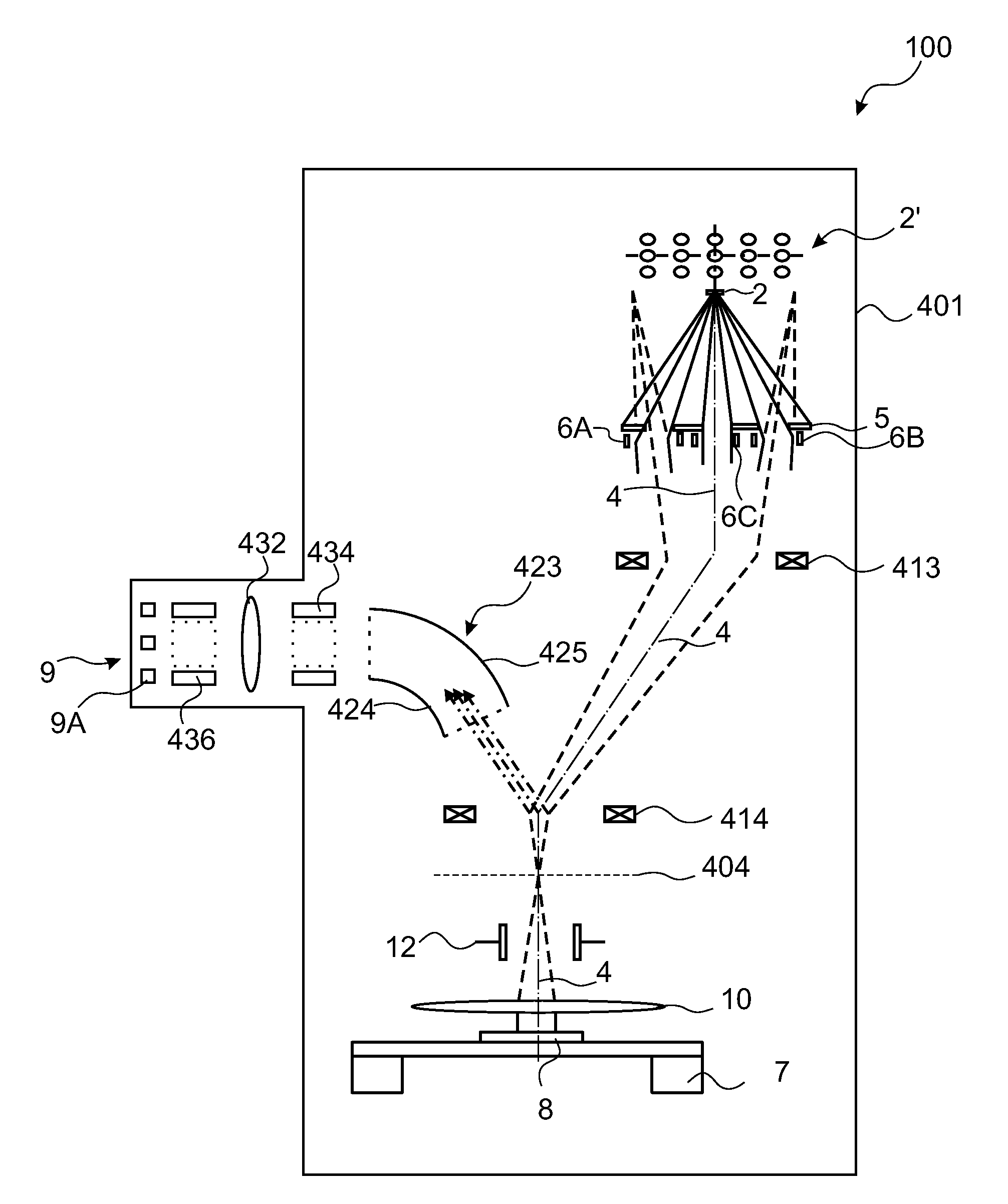
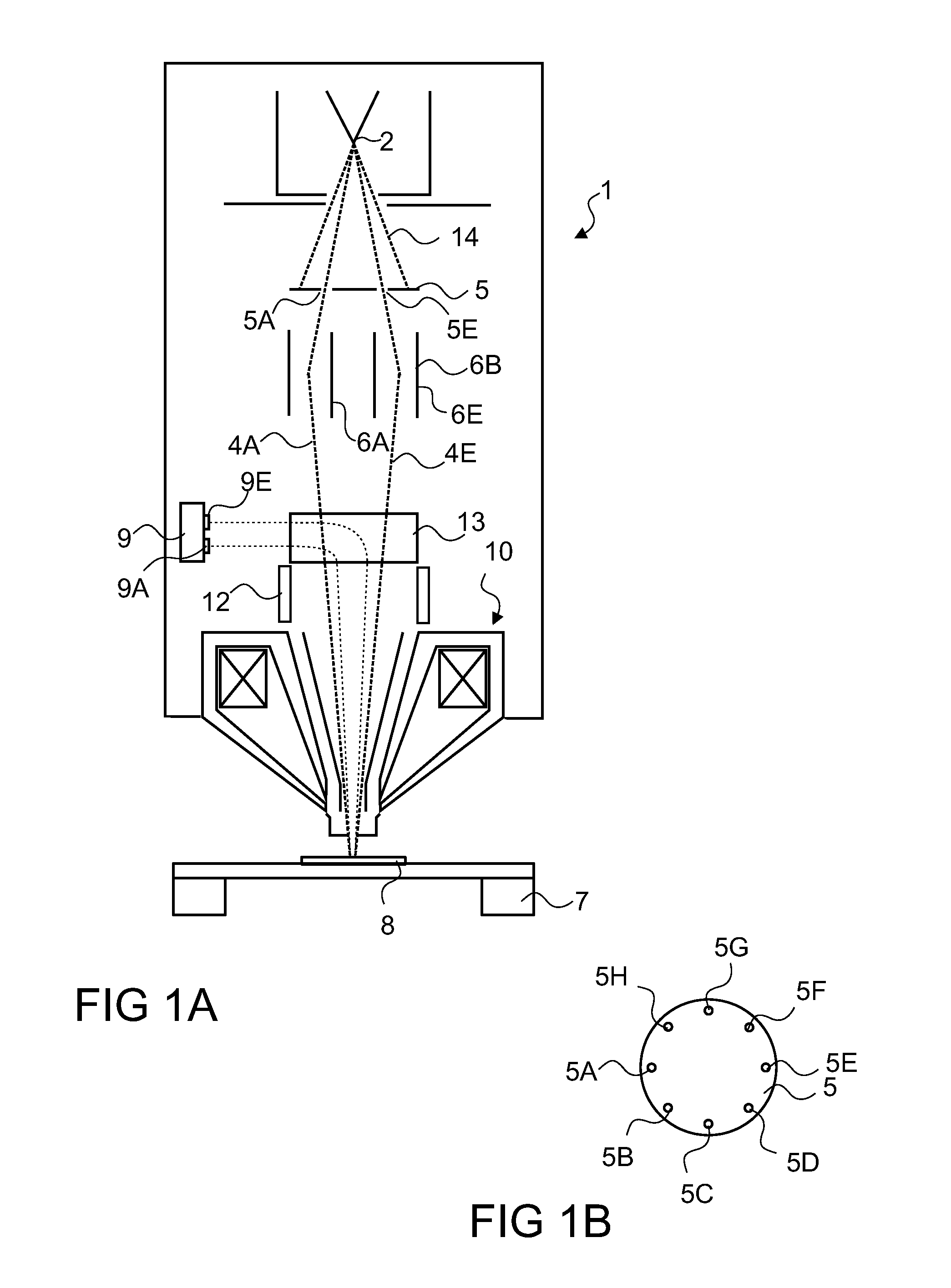
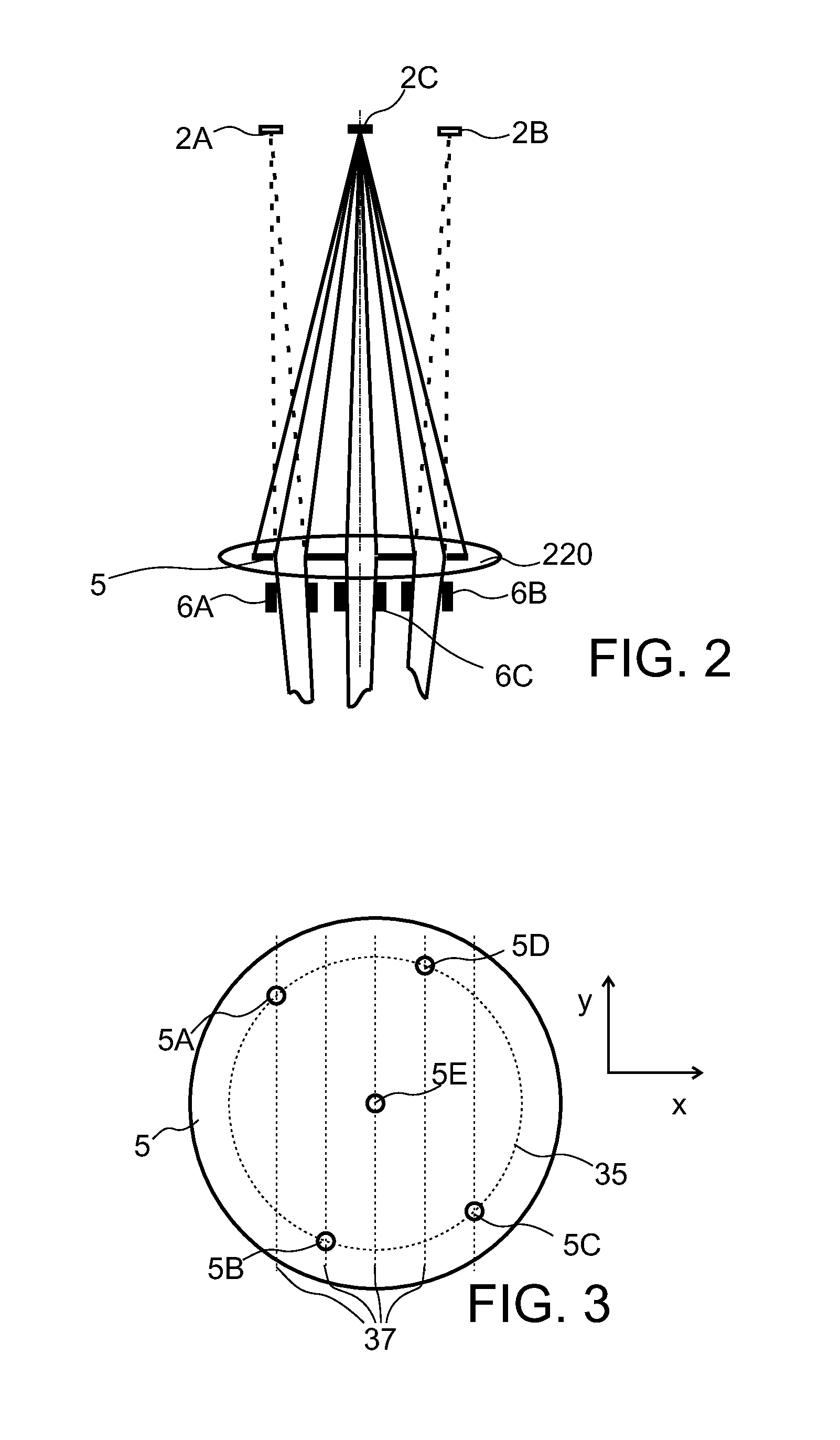
[0030]Without limiting the scope of protection of the present application, in the following the charged particle beam device or components thereof will exemplarily be referred to as a charged particle beam device including the detection of secondary electrons. Embodiments of the present invention can st...


PUM


Abstract

A scanning charged particle beam device configured to image a specimen is described. The scanning charged particle beam device includes a source of charged particles, a condenser lens for influencing the charged particles, an aperture plate having at least two aperture openings to generate at least two primary beamlets of charged particles, at least two deflectors, wherein the at least two deflectors are multi-pole deflectors, a multi-pole deflector with an order of poles of 8 or higher, an objective lens, wherein the objective lens is a retarding field compound lens, a beam separator configured to separate the at least two primary beamlets from at least two signal beamlets, a beam bender, or a deflector or a mirror configured to deflect the at least two signal beamlets, wherein the beam bender is a hemispherical beam bender or beam bender having at least two curved electrodes, and at least two detector elements.

Description

FIELD OF THE INVENTION[0001]Embodiments of the invention relate to charged particle beam devices, for example, for inspection system applications, testing system applications, defect review or critical dimensioning applications or the like. It also relates to methods of operation thereof. More particularly, embodiments relate to charged particle beam devices being multi-beam systems for high throughput EBI. Specifically, embodiments relate to a scanning charged particle beam device and a method of electron beam inspection with a scanning charged particle beam device.BACKGROUND OF THE INVENTION[0002]Modern semiconductor technology is highly dependent on an accurate control of the various processes used during the production of integrated circuits. Accordingly, the wafers have to be inspected repeatedly in order to localize problems as early as possible. Furthermore, a mask or reticle should also be inspected before its actual use during wafer processing in order to make sure that the...

Claims


Application Information

Patent Timeline
Patent Type & Authority Patents(United States)
IPC IPC(8): H01J37/28H01J37/244H01J37/147
CPCH01J37/28H01J37/1474H01J37/244H01J2237/21H01J2237/2448H01J2237/2806H01J37/05H01J37/09H01J37/1472H01J2237/0453H01J2237/0475H01J2237/1205H01J2237/24592H01J2237/2817
Inventor FROSIEN, JURGENWINKLER, DIETERCOOK, BENJAMIN JOHN
Owner ICT INTEGRATED CIRCUIT TESTING GESELLSCHAFT FUER HALBLEITERPRUEFTECHNIK GMBH
Why Eureka
Try Eureka