Method for isotropic etching

a technology of isotropic etching and etching, which is applied in the field of etching techniques, can solve the problems of affecting the etching quality of carbon-doped boron masks, and the appearance of defects that normally occur with carbon-doped masks, so as to reduce mask distortions, increase productivity, and selectivity significantly higher

Active Publication Date: 2015-06-09
COMMISSARIAT A LENERGIE ATOMIQUE ET AUX ENERGIES ALTERNATIVES +1
View PDF4 Cites 5 Cited by
  • Summary
  • Abstract
  • Description
  • Claims
  • Application Information

AI Technical Summary

Benefits of technology

[0012]It has been found that the use of such a carbon-doped boron hard mask in an inductive-coupling plasma reactor makes it possible to reduce the mask distortions that occur with the solutions using a carbon mask, makes it possible to carry out a highly anisotropic etching of said layer to be etched and makes it possible to perform all the steps in the same reactor, which increases productivity. It turns out that the selectivity in the etching of the carbon-doped boron mask is significantly higher that the selectivity in the etching of a carbon mask. Thus, during the etching of said layer to be etched, the carbon-doped boron mask is consumed much less quickly, typically at a third of the rate, than a carbon mask. As a result the thickness of the carbon-doped boron mask may be reduced compared with a carbon mask while carrying out an etching of said layer to be etched that is highly anisotropic. It has been observed that the defects that normally occur with carbon masks, such as the folding of the thin carbon patterns, appear all the more easily, the greater the thickness of the carbon mask. The invention, by making it possible to reduce the thickness of the mask through which said layer to be etched is etched, therefore reduces the defects appearing at the mask.

Problems solved by technology

It has been observed that the defects that normally occur with carbon masks, such as the folding of the thin carbon patterns, appear all the more easily, the greater the thickness of the carbon mask.

Method used


Image

  • Method for isotropic etching
  • Method for isotropic etching
  • Method for isotropic etching

Examples


Embodiment Construction

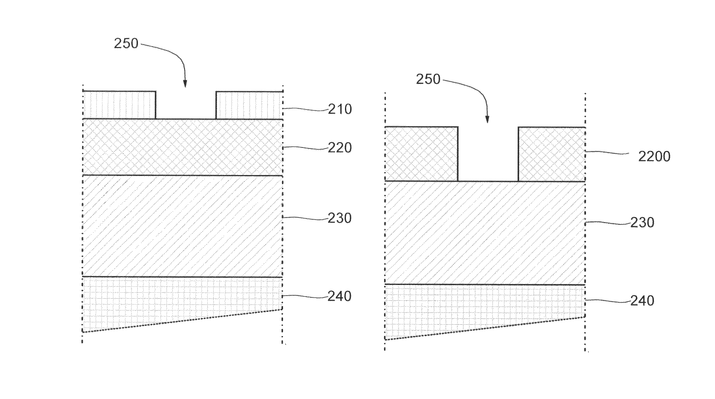
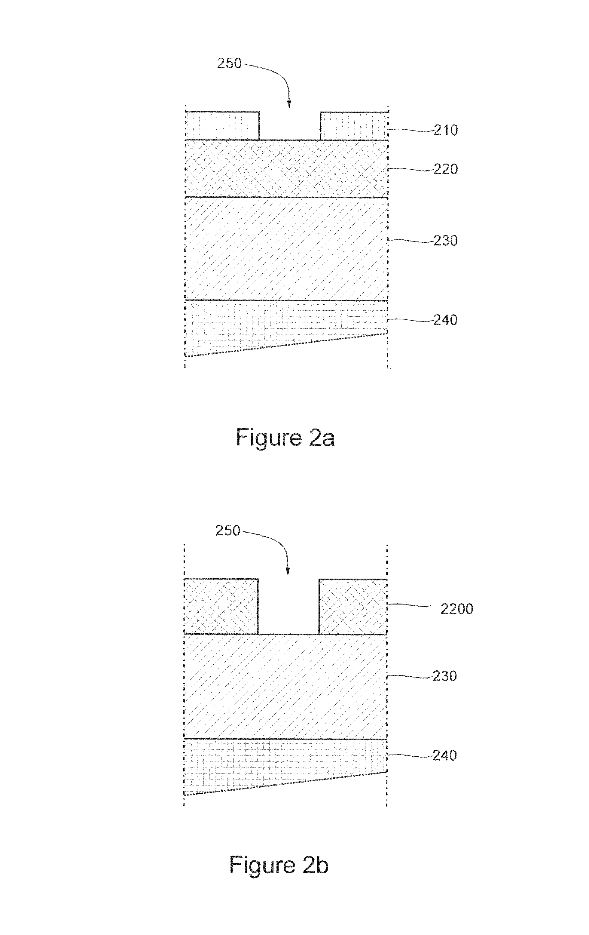
[0021]In the context of the present invention, the term “on”, “surmounts” or “underlying” or the equivalents thereof do not necessarily mean “in contact with”. Thus, for example, the deposition of a first layer on a second layer does not necessarily mean that the two layers are directly in contact with each other but means that the first layer at least partially covers the second layer while being either directly in contact therewith or being separated therefrom by another layer or another element.

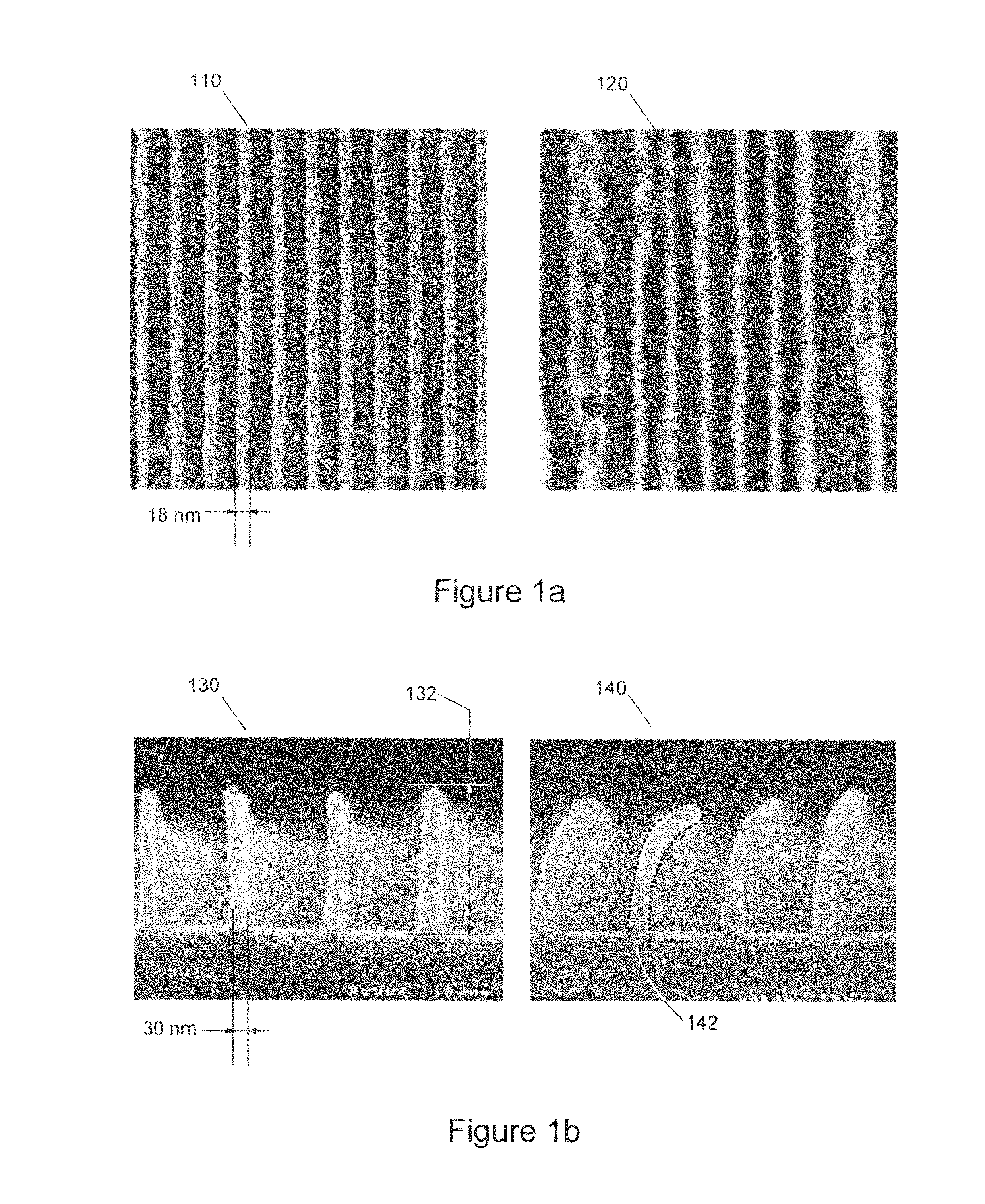
[0022]In the context of the present invention, a hard mask usually means a mask realised from a material that is not eliminated when resist masks normally used in the art are eliminated. A hard mask is differentiated from a polymer mask or a mask formed by a layer of resist which, after development, makes it possible to transfer patterns into a layer that underlies it. The hard mask is disposed between the resist mask and the layer to be etched. A hard mask is normally an inorganic mask. I...


PUM

PropertyMeasurementUnit
temperatureaaaaaaaaaa
widthaaaaaaaaaa
thicknessaaaaaaaaaa

Abstract

According to one embodiment, the invention relates to a method for the anisotropic etching of patterns in at least one layer to be etched through a hard mask comprising carbon in an inductive-coupling plasma etching reactor (ICP), the method being characterized in that the hard mask is made from boron doped with carbon (B:C), and in that, prior to the anisotropic etching of the patterns in said layer to be etched through the hard mask of carbon-doped boron (B:C), the following steps are performed:realization of an intermediate hard mask situated on a layer of carbon-doped boron intended to form the hard mask made from carbon-doped boron (B:C),etching of the layer of carbon-doped boron (B:C) through the intermediate hard mask in order to form the hard mask made from carbon-doped boron (B:C),the realization of the intermediate hard mask and the etching of the hard mask made from carbon-doped boron (B:C) being done in said inductive coupling plasma etching reactor (ICP).

Description

TECHNICAL FIELD OF THE INVENTION[0001]The present invention concerns in general the techniques of etching used in microelectronics and more particularly those based on the use of a hard mask in a plasma etching reactor.PRIOR ART[0002]The constant reduction of the dimensions of the patterns that it is necessary to be able to etch in order to produce ever denser integrated circuits has been able to be maintained only by constantly improving the techniques of photolithography and etching of the layers of materials used to realize the electronic integrated circuits. Whereas the families of integrated circuits or technological “nodes” now reach sizes of a few tens of nanometers (nm=10−9 meters), it is necessary to be able to extend the decrease in dimensions beyond the technological nodes that have succeeded each other in the past years: 90, 65 and 45 nm up to the node currently in production in the most recent lines, that is to say 32 nm.[0003]Thus, in order to reach the above decananom...

Claims


Application Information

Patent Timeline
Patent Type & Authority Patents(United States)
IPC IPC(8): H01L21/308H01L21/311H01L21/3213
CPCH01L21/3086H01L21/3081H01L21/31122H01L21/31144H01L21/32139
Inventor POSSEME, NICOLASLEE, GENE
Owner COMMISSARIAT A LENERGIE ATOMIQUE ET AUX ENERGIES ALTERNATIVES
Why Eureka
Try Eureka