Integrated circuit with electromagnetic energy anomaly detection and processing

a technology of electromagnetic energy anomaly detection and processing, applied in the field of integrated circuits, can solve the problems of counterfeit electronic and electrical components found their way into the supply chain in increasing numbers, counterfeiting occurs at the level of circuit boards, devices, boards, and fully assembled products, and achieves the effect of constant monitoring

Active Publication Date: 2015-06-16
NOKOMIS
View PDF57 Cites 33 Cited by
  • Summary
  • Abstract
  • Description
  • Claims
  • Application Information

AI Technical Summary

Benefits of technology

[0015]This present invention discloses novel application of utilizing unintended emissions to detect anomalous circuit characteristics that can be caused intentionally (e.g., substituting counterfeit parts for genuine or authentic parts; tampering with a genuine device to introduce unauthorized functionality; replacing genuine functionality with stub functionality) in a miniaturized and integrated fashion or unintentionally such as aging of parts by natural or intentionally induced processes, part degradation that may be induced environmentally or due to special events. As miniaturization and integration becomes more successful, it allows for this additional capability to be incorporated into new devices and to add this constant monitoring capability to existing devices by taking advantage of unused space that was heretofore unusable. Miniaturization also makes parts more susceptible to aging, environmental effects and damage from events such as reverse polarity, lightning strikes etc., making this technology more important as the protected and protective devices co-miniaturize.

Problems solved by technology

The components used in circuit boards are especially susceptible to counterfeiting and tampering.
Counterfeit electronic and electrical components have found their way into the supply chain in increasing numbers.
Counterfeiting occurs at the die, part, device, board and fully assembled product level.
However, a solution has not existed to detect if a counterfeit component was introduced onto a circuit board during rework or to have an on-board mechanism that could detect the installation of a counterfeit whether that counterfeit was introduced during the manufacturing process or at a later stage.
Prior to the instant invention all of the techniques are either superficial or extremely expensive and none of them are installed in-situ with the circuitry that needs to be monitored.
Of superficial techniques, the simplest is visual inspection, but as counterfeits have become increasing sophisticated these techniques have become less reliable.
In contrast, reliable techniques that are in existence are expensive or are destructive in nature.
FIBs are inherently destructive as they irrevocably affect the crystalline structure of the die on which they are used, and result in an amorphous structure when used for deeper milling, especially with silicon.
From a computational point of view, these modifications may not necessarily affect the noticeable digital operation of the device in question, though they certainly could introduce additional delays, and affect timing constraints.
From the point of view of electromagnetic emissions, however, these introduced defects are precisely the sort of things that affect trace (and consequently radiator) length, engineered electromagnetic interference (EMI) protection, grounding and terminating resistors, carefully controlled transistor junction length and transconductance, specific dielectric permittivity, isolation of intentionally suppressed or inherent low-level electromagnetic emissions, etc.
In fact, even effects introduced by inherent process variations are so pronounced within modern technology nodes that the modeling and iterative analysis to control these effects are now considered the most difficult element of the design process.

Method used


Image

  • Integrated circuit with electromagnetic energy anomaly detection and processing
  • Integrated circuit with electromagnetic energy anomaly detection and processing
  • Integrated circuit with electromagnetic energy anomaly detection and processing

Examples


Embodiment Construction

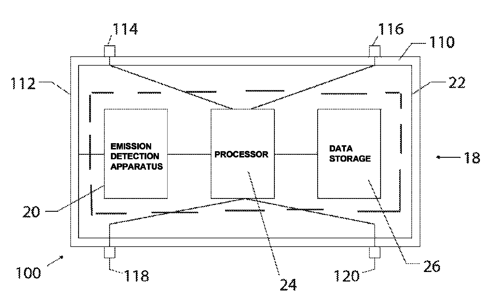
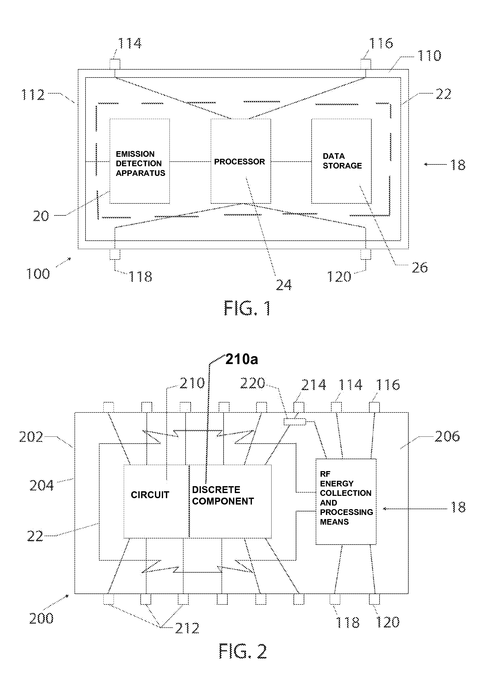
[0059]Prior to proceeding to the more detailed description of the present invention it should be noted that, for the sake of clarity and understanding, identical components which have identical functions have been identified with identical reference numerals throughout the several views illustrated in the drawing figures.

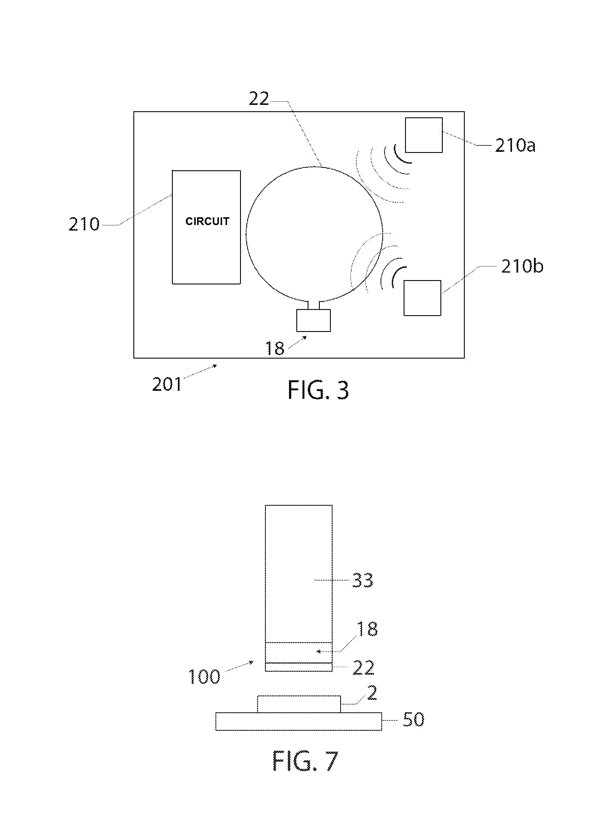
[0060]For the sake of reader's convenience, the following description is repeated from the co-pending U.S. Ser. No. 13 / 410,797 entitled “SYSTEM AND METHOD FOR PHYSICALLY DETECTING COUNTERFEIT ELECTRONICS”, published as U.S. Pub. No. 2012-0226463 A1 on Sep. 6, 2012. Now in a reference to FIGS. 8-11, there is provided a system, generally designated as 10, for differentiating between a counterfeit and genuine condition of an electrically powered device 2. The device 2 includes but is not limited to at least one of a discrete component, integrated circuit (IC), circuit board, circuit board assembly populated with electronic components, subsystem, system, electronic devi...


PUM


Abstract

An integrated circuit includes an antenna, a die manufactured from a semiconducting material, an RF energy collection and processing device disposed on or within the die and including at least a receiver and a processing device, an input configured to supply power to said RF energy collection and processing device and an output for operative communication by said RF energy collection and processing device. The integrated circuit is configurable and operable to provide at least one of electromagnetic emission anomaly detection, tamper detection, anti-tamper monitoring, degradation monitoring, health monitoring, counterfeit detection, software changes monitoring, firmware changes monitoring and monitoring of other RF energy anomalies.

Description

CROSS REFERENCE TO RELATED APPLICATION[0001]This patent application is related to and claims priority from U.S. Provisional Patent Application Ser. No. 61 / 464,262 filed Mar. 2, 2011 and U.S. Provisional Patent Application Ser. No. 61 / 574,250 filed Jul. 29, 2011 respectively and being incorporated into this document by reference thereto. This application is further closely related to a co-pending U.S. Ser. No. 13 / 410,797 entitled “SYSTEM AND METHOD FOR PHYSICALLY DETECTING COUNTERFEIT ELECTRONICS”, published as U.S. Pub. No. 2012-0226463 A1 on Sep. 6, 2012. This application is being assigned to the assignee of the present invention and the disclosure of this co-pending application is hereby incorporated by reference thereto.STATEMENT REGARDING FEDERALLY SPONSORED RESEARCH AND DEVELOPMENT[0002]N / AREFERENCE TO SEQUENCE LISTING, A TABLE, OR A COMPUTER PROGRAM LISTING COMPACT DISC APPENDIX[0003]N / AFIELD OF THE INVENTION[0004]The present invention relates, in general, to integrated circui...

Claims


Application Information

Patent Timeline
Patent Type & Authority Patents(United States)
IPC IPC(8): G08B13/14H01L23/00
CPCH01L23/576H01L2223/6677H01L2924/14H01L2924/19105H01L2924/0002H01L2924/00G06F21/44G06F21/76G06F21/87H01L23/66H04B1/26
Inventor KELLER, III, WALTER J.PATHAK, BOGDAN A.
Owner NOKOMIS
Why Eureka
Try Eureka