Super junction field effect transistor

Active Publication Date: 2015-07-14
LITTELFUSE INC
View PDF3 Cites 31 Cited by
  • Summary
  • Abstract
  • Description
  • Claims
  • Application Information

AI Technical Summary

Benefits of technology

[0003]A split-body Super Junction Field Effect Transistor (FET) device includes a charge compensation region disposed on a substrate of monocrystalline semiconductor material. The charge compensation region includes a plurality of columns of P− type epitaxial semiconductor material within a region of N− type epitaxial semiconductor material. The column may, for example, be stripes or cylindrical columns organized concentrically with respect to one another. The alternating P− type and N− type semiconductor material makes the charge compensation region. The concentration N type dopants in the upper portion of the N− type material of the charge compensation region is made higher, therefore forming an N− type JFET layer at the top of the charge compensation region. A thin oxide layer is disposed on an upper semiconductor surface of the JFET layer. A plurality of P type edge termination floating rings extend from the upper semiconductor surface down into the semiconductor material toward the substrate. An N++ type polysilicon gate structure is disposed on an upper surface of the thin oxide layer. An IL

Problems solved by technology

But making the concentration of N type dopants in the N type drift region low results

Method used


Image

  • Super junction field effect transistor
  • Super junction field effect transistor
  • Super junction field effect transistor

Examples


Embodiment Construction

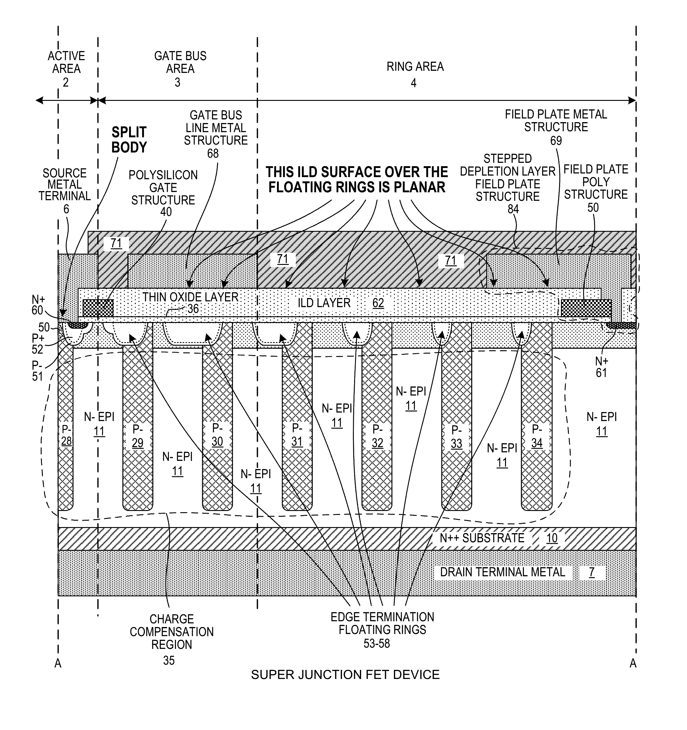
[0026]Reference will now be made in detail to some embodiments of the invention, examples of which are illustrated in the accompanying drawings. In the text and drawings, the dopant labels N++, N+, N−, N, P+, P−, and P are only very loose general descriptions of relative dopant concentrations. A particular dopant label appearing in the text below has meaning within the local context of its usage. In the text and drawings, the term P type is sometimes used not as a description of a relative dopant concentration, but rather is used as a broad term to denote semiconductor material that may be P− type, or may be P type, or may be P+ type, or that may include sub-regions of various P type dopant concentrations.

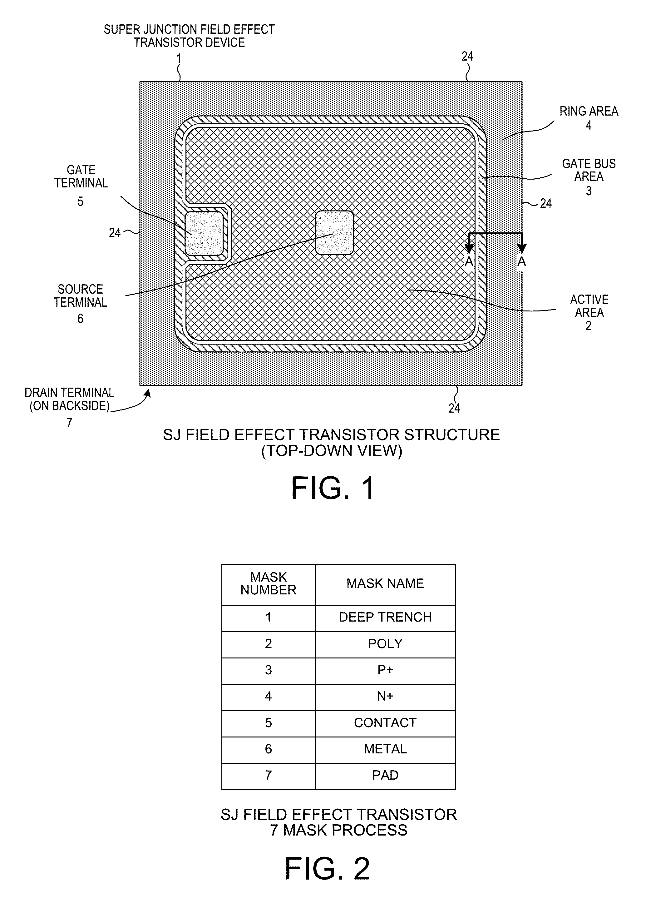
[0027]FIG. 1 is a top-down diagram of a Super Junction FET (Field Effect Transistor) device die 1 in accordance with one novel aspect. Such a Super Junction FET device 1 is also loosely referred to as a Super Junction MOSFET (Metal Oxide Semiconductor Field Effect Transistor), even...


PUM


Abstract

A split-body Super Junction FET is made using only seven masks. Thin oxide is disposed on an upper semiconductor surface of a super junction charge compensation region. A polysilicon gate is disposed on the thin oxide. An ILD (InterLayer Dielectric) layer is disposed on the upper surface of the thin oxide so that the ILD layer covers the polysilicon gate. A gate bus line metal structure and a field plate metal structure are disposed on the upper surface of the ILD. A portion of the upper surface of the ILD extends from the gate bus line metal, laterally over floating rings, and to the field plate metal. This portion of the upper surface of the ILD layer is substantially planar where the ILD layer passes over the floating rings. The field plate metal structure, a polysilicon feature, and a diffusion region together form a stepped depletion layer field plate structure.

Description

TECHNICAL FIELD[0001]The described embodiments relate generally to Super Junction field effect transistors and methods for making Super Junction field effect transistors.BACKGROUND INFORMATION[0002]To make a conventional power N-channel field effect transistor that meets a particular breakdown voltage requirement, the concentration of N type dopants in the N type drift region of the transistor must be adequately low. But making the concentration of N type dopants in the N type drift region low results in an undesirably high resistivity of the semiconductor material in the drift region. For the conventional power N-channel field effect transistor to have a required current rating (RDS(ON) is not higher than a specified value when a given current is flowing through the transistor), the die area of the conventional power N-channel field effect transistor has to be made correspondingly large in order to achieve the required low drain-to-source resistance RDS(ON) of the overall transisto...

Claims


Application Information

Patent Timeline
IPC IPC(8): H01L29/78H01L29/66H01L29/49H01L29/40H01L21/02H01L29/06
CPCH01L29/7811H01L29/0634H01L29/402H01L29/4916H01L29/66712H01L29/0619H01L21/02129H01L29/0638
Inventor SEOK, KYOUNG WOOK
Owner LITTELFUSE INC
Why Eureka
Try Eureka