Methods for manufacturing isolated deep trench and high-voltage LED chip

a technology of led chips and deep trenches, which is applied in the direction of basic electric elements, electrical equipment, semiconductor devices, etc., can solve the problems of shortening the service life of the chip, increasing the probability of light being absorbed, and affecting the reliability of the devi

Inactive Publication Date: 2015-07-14
ENRAYTEK OPTOELECTRONICS
View PDF13 Cites 0 Cited by
  • Summary
  • Abstract
  • Description
  • Claims
  • Application Information

AI Technical Summary

Benefits of technology

[0009]An objective of the present invention is to provide a method of forming deep isolation trenches and a method of forming a high-voltage LED chip to reduce the cost of forming the deep trenches of the HV LED chip and ensure sufficient continuity and compactness of insulating, isolating dielectric layers and interconnecting contact layers within the deep trenches.
[0024]It can be understood from the foregoing description that, compared with the conventional processes for forming deep isolation trenches between micro cells of a HV LED chip, the methods of the present invention are performed by depositing a mask layer over a sapphire substrate, forming, by photolithography and etching, a plurality of windows which are isolated from one another and each of the windows exposes the underlying substrate, and forming, by an ELOG process, the micro cells of the HV LED chip as trapezoid-shaped epitaxial structures, each filling, and covering part of the mask layer surrounding, a corresponding one of the windows, the space between each pair of adjacent ones of the epitaxial structures automatically forming the first deep trench. Since the width, sidewall slope and width-to-depth ratio of the first deep trench is adjustable by changing a pattern width or a thickness of the mask layer, or changing parameters of the ELOG process, HV LED chips with different geometric profiles of the first deep trench can be realized. The ELOG process enables the automatic formation of the deep isolation trenches and thus eliminates the need for adopting multiple ICP etching processes, and the methods can be used in the fabrication of any other LED chip which incorporates a plurality of interconnected LED cells.

Problems solved by technology

This requires the device to have a good equilibrium between its P- and N-side electrodes, because any defective equilibrium will lead to significant current crowding, which can cause droop effect with the temperature rising around the electrodes, hence impinging the reliability and shortening the service life of the chip.
On the other hand, it is a great challenge to homogenize distribution of the current density over the HP LED chip to mitigate the current crowding.
Further, due to the geometric nature of the chip, the longer distance light travels in the chip, the more likely the light is to be absorbed.
Therefore, a horizontal HP LED chip composed of large-die LEDs typically has lower light extraction efficiency than the one composed of small-die LEDs.
This complicates the manufacture, leads to a lower yield than that of the horizontal device, and raises the cost.
While the HV LED chip made by this method has good heat dissipation performance, unreliable interconnection of the conductive wires remains a problem.
Any loose or broken solder joint will lead to failure of the whole HV LED chip.
It can be concluded from the aforementioned processes that the formation of the deep trenches between the micro cells of the HV LED chip involves deposition of a hard mask and performance of an ICP etching process, which leads to great process complexity, and in particular, the multiple ICP etching processes inevitably introduce impairment to the epitaxial layer, thus adversely affecting the process cost and yield.
In addition, while there is generally no specific requirement imposed on the width of the deep trenches, considering the obvious fact that too larger trench width will lead to a smaller effective emitting area and hence lower performance of the LED chip, it is desirable for these processes to have a capability of forming the deep trenches with a large ratio of depth to width.
However, the trench width is hard to be reduced.
Furthermore, in order to ensure sufficient continuity and compactness of insulating, isolating dielectric layers and interconnecting contact layers within the deep trenches, the sidewalls of the trenches etched by the ICP process is required to have a suitable slope, which is indeed a challenging task.

Method used


Image

  • Methods for manufacturing isolated deep trench and high-voltage LED chip
  • Methods for manufacturing isolated deep trench and high-voltage LED chip
  • Methods for manufacturing isolated deep trench and high-voltage LED chip

Examples


Embodiment Construction

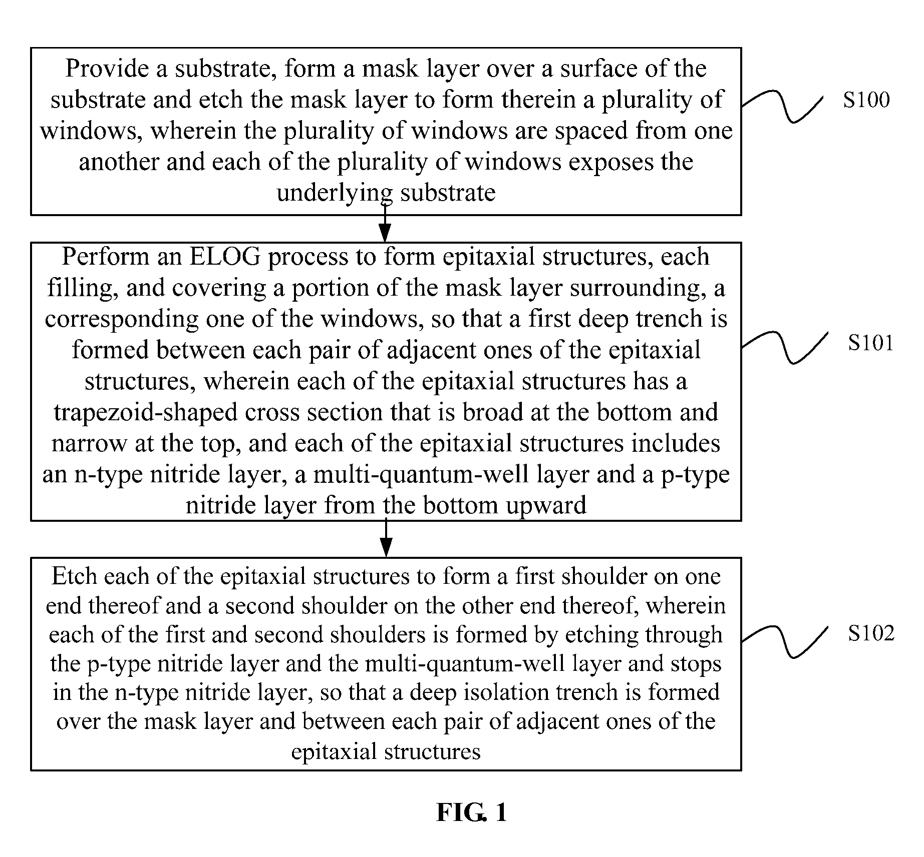
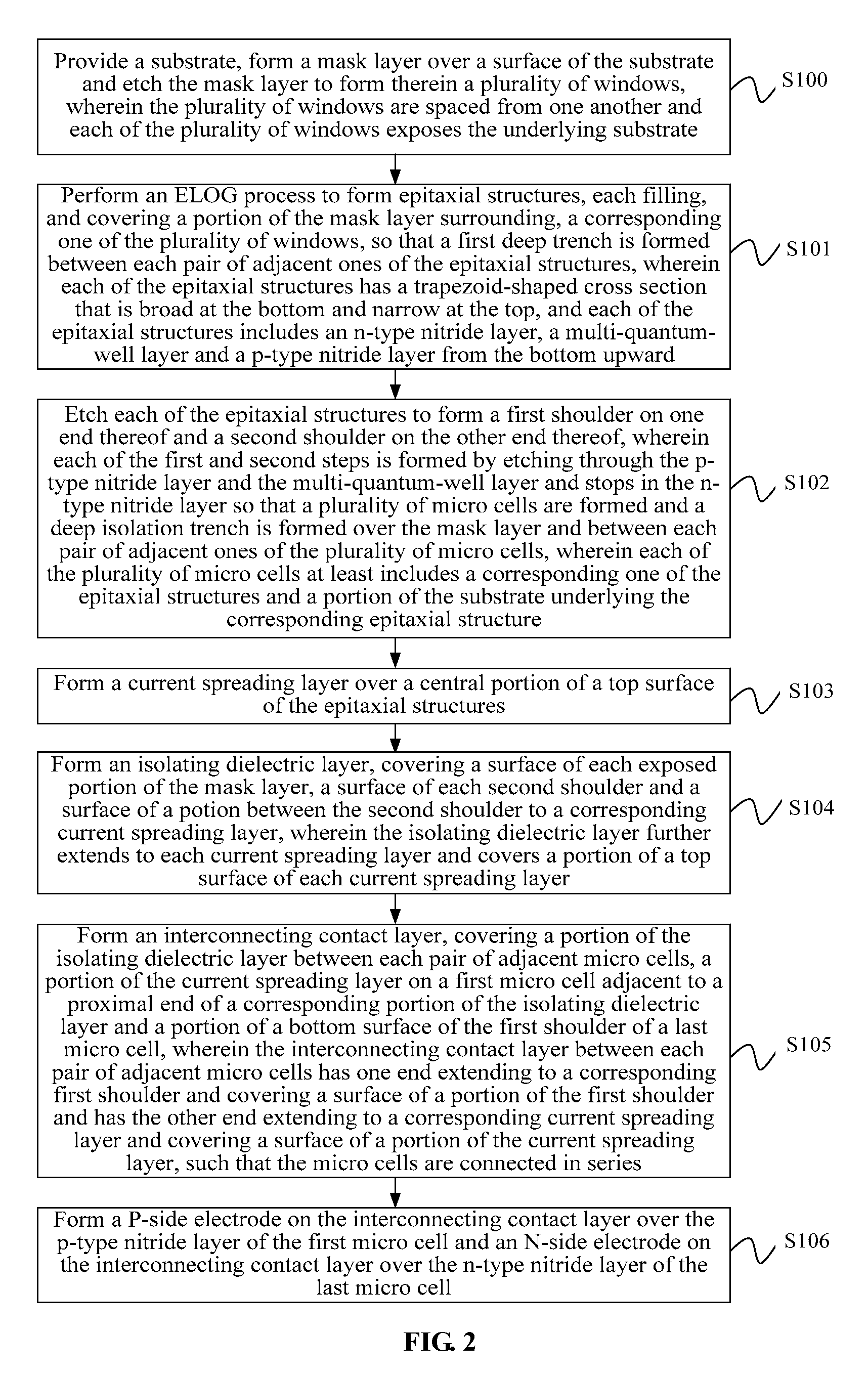
[0028]The above and other objectives, advantages and salient features of the invention will become apparent from the following detailed description, which, taken in conjunction with the accompanying drawings, discloses preferred embodiments of the invention.

[0029]The embodiments are intended to describe aspects of the invention in sufficient detail. Other embodiments can be utilized and changes can be made by those skilled in the art without departing from the scope of the present invention. The following detailed description of the invention is, therefore, not to be taken in a limiting sense.

[0030]In addition, the accompanying drawings are schematic representations only and of which the cross-sectional views illustrative of the various steps may not be drawn to common scale, but partially enlarged for the sake of clarity in explaining the preferred embodiments. These schematic representations are exemplary configurations and they are not intended to be limiting. Further, while omit...


PUM


Abstract

A method for manufacturing a deep isolation trench (221) and a method for manufacturing a high-voltage LED chip. Steps of the method for manufacturing a deep isolation trench (221) are as follows: forming a mask layer (202) on a substrate (200), and forming, in the mask layer, through etching, multiple windows (204) isolated from each other, the bottom of each window exposing the substrate; with epitaxial lateral overgrowth, forming an epitaxial structure (212) inside each window and a part of the mask layer around the window, respectively, each epitaxial structure having a trapezoidal cross section with a long bottom and a short top, and a gap between adjacent epitaxial structures forming a first deep trench (214); etching each epitaxial structure, forming a first shoulder (218) and a second shoulder (221) at both sides of each epitaxial structure, respectively, and forming a deep isolation trench above the mask layer between the adjacent epitaxial structures. The method for manufacturing a high-voltage LED chip is capable of decreasing preparation cost of the deep isolation trench in the high-voltage LED chip, and increasing continuity and compactness interconnection performance of an insulation isolation dielectric layer and an interconnection electrode layer between deep isolation trenches within a high-voltage LED chip.

Description

TECHNICAL FIELD[0001]The present invention relates generally to the fabrication of light-emitting devices, and in particular to a method of forming deep isolation trenches and a method of forming a high-voltage LED chip incorporating the deep isolation trenches.BACKGROUND[0002]With the rapid development of semiconductor integration technology and the enhancement of electron-to-photon conversion efficiency, light-emitting diodes (LEDs) fabricated from nitrides of Group III materials have been widely used. In addition, with the diversification of applications and the increase of market demand, high-power, high-brightness LED chips are gaining more and more popularity.[0003]Most of the existing high-power (HP) LED chips are still based on conventional large-die, low-voltage, direction-current (DC) LEDs and are grouped into horizontal and vertical structures. Compared with LED chips composed of small-die LEDs, a horizontal HP LED chip composed of large-die LEDs is usually required to op...

Claims


Application Information

Patent Timeline
Patent Type & Authority Patents(United States)
IPC IPC(8): H01L21/00H01L33/00H01L21/36H01L21/20H01L27/15H01L33/42H01L33/06H01L33/44H01L21/02H01L33/62H01L33/20
CPCH01L33/0075H01L27/156H01L33/06H01L33/42H01L33/44H01L21/0254H01L21/02458H01L21/02647H01L33/007H01L33/20H01L33/62H01L2924/0002H01L2933/0016H01L2933/0025H01L2933/0033H01L2924/00H01L33/0095
Inventor YAO, LUJUNXIAO, DEYUANCHANG, RICHARD RU-GINYU, HONGBO
Owner ENRAYTEK OPTOELECTRONICS
Why Eureka
Try Eureka