Semiconductor device

a technology of semiconductors and devices, applied in the direction of semiconductor devices, electrical equipment, transistors, etc., can solve the problems of local breakdown, difficult to secure, local breakdown,

Inactive Publication Date: 2015-09-15
ABLIC INC
View PDF5 Cites 8 Cited by
  • Summary
  • Abstract
  • Description
  • Claims
  • Application Information

AI Technical Summary

Benefits of technology

[0010]In an N-type MOS transistor for ESD protection having an integral structure of a plurality of transistors in which a plurality of drain regions and a plurality of source regions are alternately formed, a gate electrode is formed between each of the drain regions and each of the source regions, and a substrate contact for fixing a potential of the gate electrode to a ground potential is formed on a guard ring around an outer periphery, the drain regions are electrically connected to an external connection terminal and the source regions are electrically connected to a ground potential supply line, and a length L of a single comb tooth of the gate electrode is reduced as the distance from the substrate contact, whose potential is fixed at the ground potential and provided around the outer periphery, becomes smaller, and is increased as the distance becomes larger.
[0011]According to one embodiment of the present invention, by increasing the L length of the gate electrode as the distance from the substrate contact whose potential is fixed at the ground potential becomes larger, that is, as the comb tooth of the gate electrode is located more inward, the respective comb teeth of the gate electrode uniformly enter snap-back operation, which enables avoidance of local concentration of current and obtainment of a desired ESD tolerance.

Problems solved by technology

However, due to the structure in which a plurality of transistors are combined, it is difficult for the entire MOS transistor for ESD protection to operate uniformly, and there is a problem in that only a comb tooth which first enters parasitic bipolar operation cannot receive the entire ESD surge, resulting in local breakdown.
Accordingly current concentrates on the unit ESD protection element having the parasitic bipolar transistor which has been turned on the earliest, resulting in local breakdown.
However, the above-mentioned method has problems in that, as the width of the drain region is reduced, it becomes more difficult to secure a desired position of the contact, and, as the resistance of the interconnecting line becomes lower due to the interconnecting line containing a high-melting point metal in recent years, the propagation speed of the surge becomes further faster, and there are cases in which only the distance between the contact and the gate electrode cannot make a complete adjustment.

Method used


Image

  • Semiconductor device
  • Semiconductor device
  • Semiconductor device

Examples


first embodiment

[0017]FIG. 1 is a schematic plan view illustrating an N-type MOS transistor for ESD protection of a semiconductor device according to a first embodiment of the present invention.

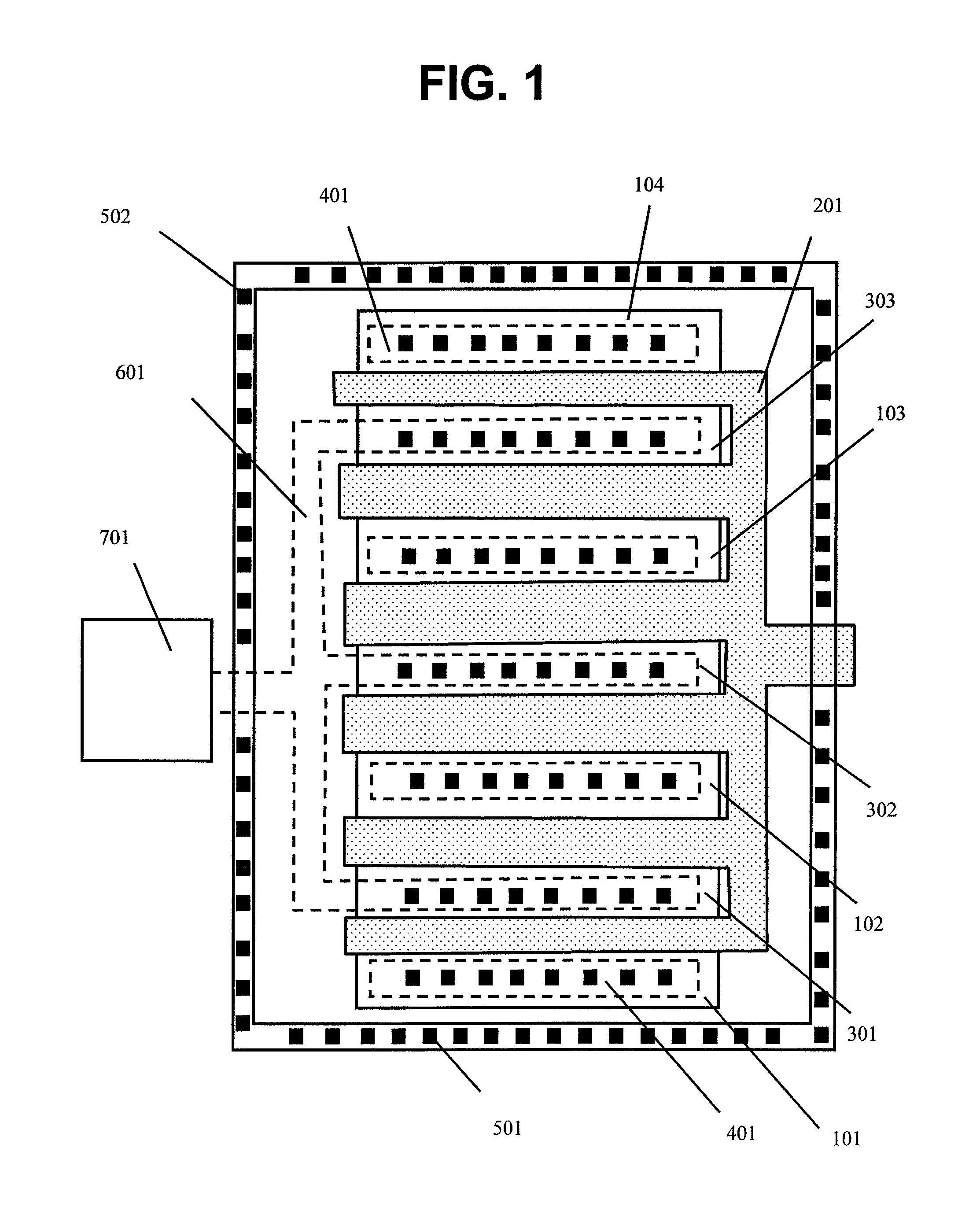
[0018]A first source region 101 and a first drain region 301, which are N-type high concentration impurity regions, are formed. A gate insulating film, which is a silicon oxide film or the like, is provided between the first source region 101 and the first drain region 301. A gate electrode 201 formed of polysilicon or the like is formed on an upper surface of the gate insulating film. A second source region 102 is formed next to the first drain region 301 with the gate electrode 201 interposed therebetween. A second drain region 302 is formed next to the second source region 102 with the gate electrode 201 interposed therebetween. In a pattern in which the above is repeated similarly, a third source region 103, a third drain region 303, and a fourth source region 104 are formed with the electrode 201 interp...

second embodiment

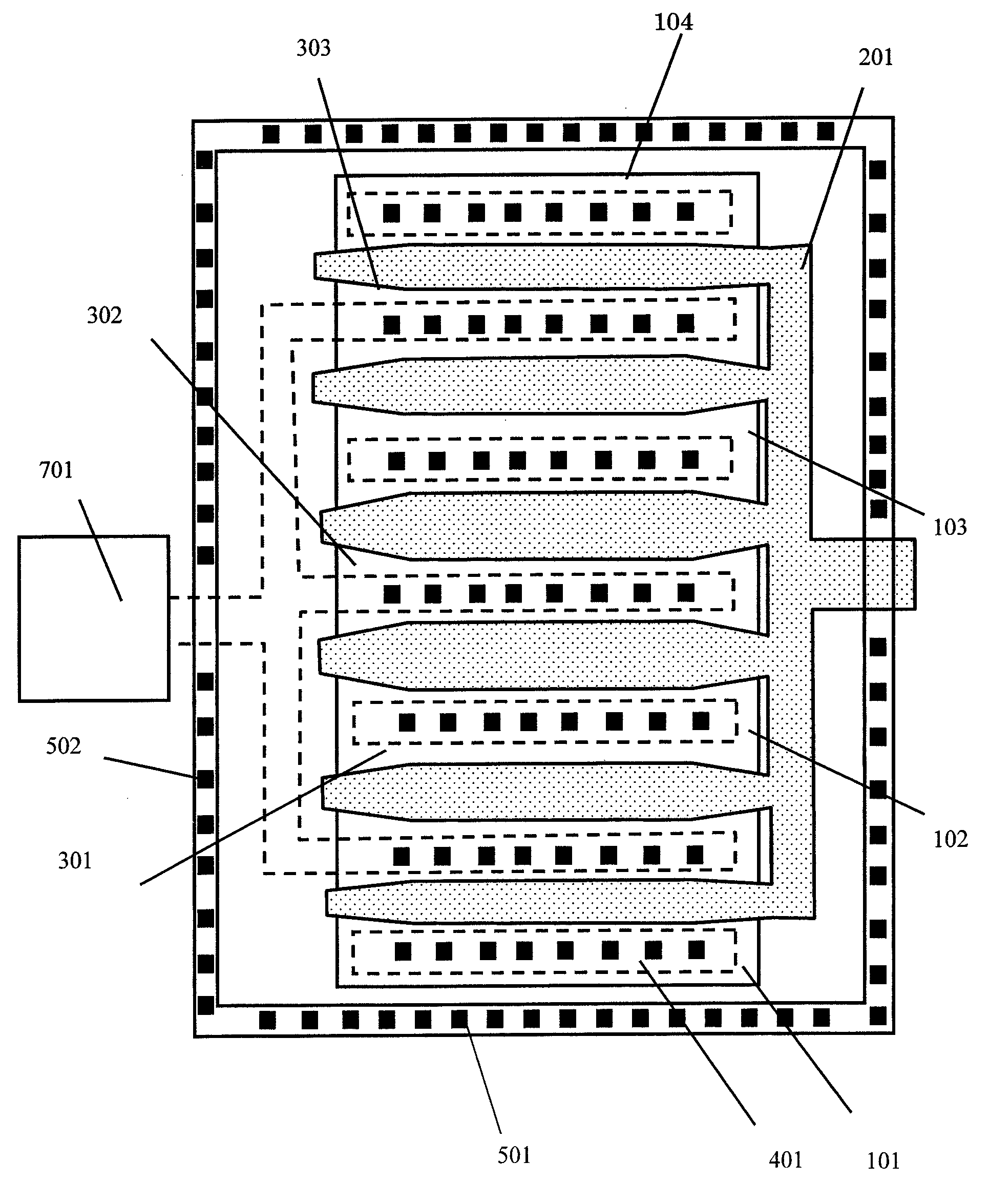
[0021]FIG. 2 is a schematic plan view illustrating an N-type MOS transistor for ESD protection of a semiconductor device according to a second embodiment of the present invention. Like reference numerals are used to designate members corresponding to those illustrated in FIG. 1. The second embodiment is different from the first embodiment illustrated in FIG. 1 in that the length L of the unit gate electrode is not fixed. In FIG. 2, not only the substrate contacts 501 arranged in the direction in parallel with the channel width which is the lateral direction in the figure but also the substrate contacts 502 arranged in the direction in parallel with the channel length which is a longitudinal direction in the figure are provided. In consideration of this, the lengths L around distal ends and proximal ends at which the distance to the substrate contact 502 is small of the comb teeth of the gate electrode 201 are set smaller than the lengths L around intermediate portions, respectively....

third embodiment

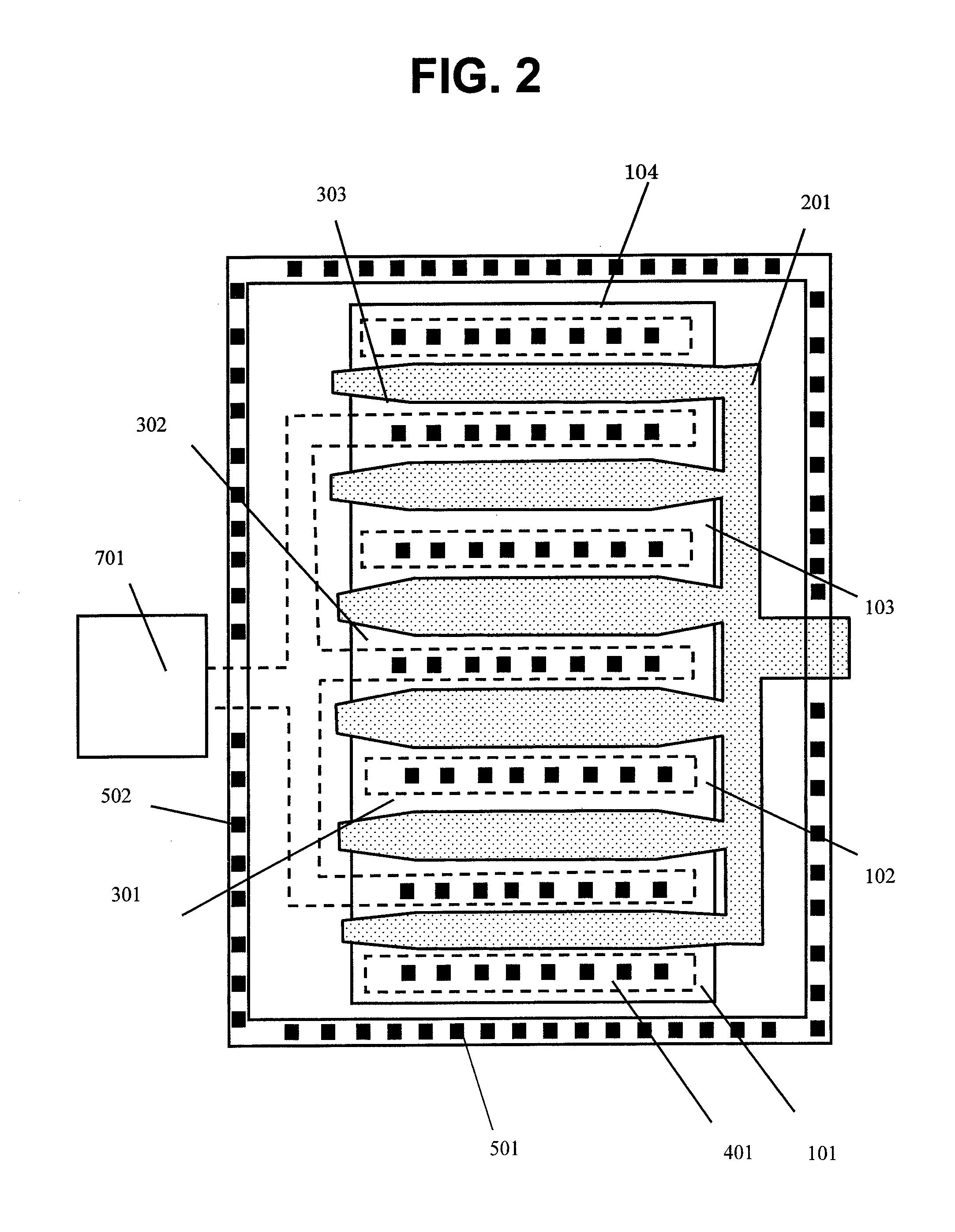
[0023]FIG. 3 is a schematic plan view illustrating an N-type MOS transistor for ESD protection of a semiconductor device according to a third embodiment of the present invention. Like reference numerals are used to designate members corresponding to those illustrated in FIG. 1. The third embodiment is different from the first embodiment illustrated in FIG. 1 in that, by omitting the substrate contacts arranged in the direction in parallel with the channel length of the N-type MOS transistor for ESD protection, the influence of difference in substrate potential in the direction in parallel with the channel length is eliminated, and only the substrate contacts 501 arranged in the direction in parallel with the channel width are provided on the guard ring around the outer periphery. The comb teeth of the gate electrode 201 in this case are provided so that, similarly to the case of the first embodiment, the length L of the comb tooth of the gate electrode is reduced as the distance fro...


PUM


Abstract

Provided is a semiconductor device which uses a comb-like N-type MOS transistor as an ESD protection element and is capable of uniformly operating the entire comb-like N-type MOS transistor. By adjusting a length L of a gate electrode of the N-type MOS transistor used as the ESD protection element in accordance with the distance from a contact for fixing a substrate potential, which is provided on a guard ring around an outer periphery, respective portion of N-type MOS transistor represented as a comb teeth uniformly enter snap-back operation, permitting avoidance of local concentration of current and obtainment of a desired ESD tolerance.

Description

BACKGROUND OF THE INVENTION[0001]1. Field of the Invention[0002]The present invention relates to a semiconductor device, in particular, to a semiconductor device using an N-type MOS transistor as an ESD protection element.[0003]2. Description of the Related Art[0004]In a semiconductor device including a MOS transistor, in order to prevent electrostatic breakdown of an internal circuit by static electricity from a pad for external connection (VDD), an off transistor provided under a state in which a gate potential of an N-type MOS transistor is fixed to a ground potential (Vss) so as to be in an off state is often used as an ESD protection element.[0005]The off transistor should have a channel width (W) which is larger than that of an ordinary internal MOS transistor structure since an off transistor must flow the entire current caused by the static electricity in a short time and in a large amount. As a result, it is often the case that the entire channel width of an off transistor ...

Claims


Application Information

Patent Timeline
Patent Type & Authority Patents(United States)
IPC IPC(8): H01L27/02
CPCH01L27/0266H01L27/0277H01L29/4238H01L29/41758
Inventor KOYAMA, TAKESHIRISAKI, TOMOMITSU
Owner ABLIC INC
Why Eureka
Try Eureka