System for separating devices from a semiconductor wafer

a technology of semiconductor wafers and separation systems, applied in semiconductor/solid-state device manufacturing, basic electric elements, electric apparatus, etc., can solve the problems of film stretching and losing tension on the mounting frame, not giving a high yield of separated devices, and back metal film breaking

Active Publication Date: 2015-10-06
SEMICON COMPONENTS IND LLC
View PDF6 Cites 7 Cited by
  • Summary
  • Abstract
  • Description
  • Claims
  • Application Information

AI Technical Summary

Benefits of technology

[0009]During the etching process, the plastic film is exposed to harsh chemicals and heat that can cause the film to stretch and lose tension on the mounting frame. In the process of this invention prior to applying the stylus to the back side of the film and wafer the film is stretched to reestablish the tension in the film. The initial approach was to stretch and tension the film as much as possible while keeping it in the regime of its elastic deformation. Surprisingly this did not give a high yield of separated devices. It was observed that before and during the application of the stylus, breaks would occur in the back metal films. These breaks are generally in lines in one or both directions between the devices and can extend for some distance, sometimes all the way to the edges of the wafer. It was found that when the plastic film was stretched a large amount before the stylus was applied, the film would deform more in the broken lines than between the adjacent devices that were not yet separated. The excess deformation in the previously broken lines prevents adequate deformation of the plastic film under the back metal in the adjacent lines and results in the metal not breaking between these devices. This dramatically reduces the yield of separated devices. This effect was observed when a stretch (strain) of 3.0% to 3.5% was applied to the film. If the stretch (strain) applied to the film is kept to a lower range of 0.5% to 1.0% this effect is avoided. It is, therefore, essential to include precise control of the plastic film stretch and tension in order to achieve high yields of die separation and to make this process economically viable.

Problems solved by technology

During the etching process, the plastic film is exposed to harsh chemicals and heat that can cause the film to stretch and lose tension on the mounting frame.
Surprisingly this did not give a high yield of separated devices.
It was observed that before and during the application of the stylus, breaks would occur in the back metal films.
It was found that when the plastic film was stretched a large amount before the stylus was applied, the film would deform more in the broken lines than between the adjacent devices that were not yet separated.
The excess deformation in the previously broken lines prevents adequate deformation of the plastic film under the back metal in the adjacent lines and results in the metal not breaking between these devices.
This dramatically reduces the yield of separated devices.
When one wishes to control the stretch and tension in the plastic film, simply moving all parts of the film outward a certain distance in a radial direction does not achieve the desired results.
In some cases, the stretch and tension in the film may be negative; that is, the film is sagging in the frame.

Method used


Image

  • System for separating devices from a semiconductor wafer
  • System for separating devices from a semiconductor wafer
  • System for separating devices from a semiconductor wafer

Examples


first embodiment

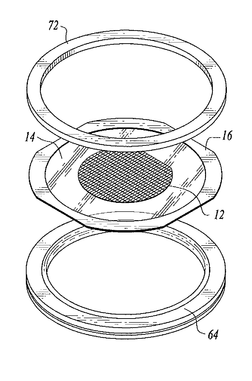
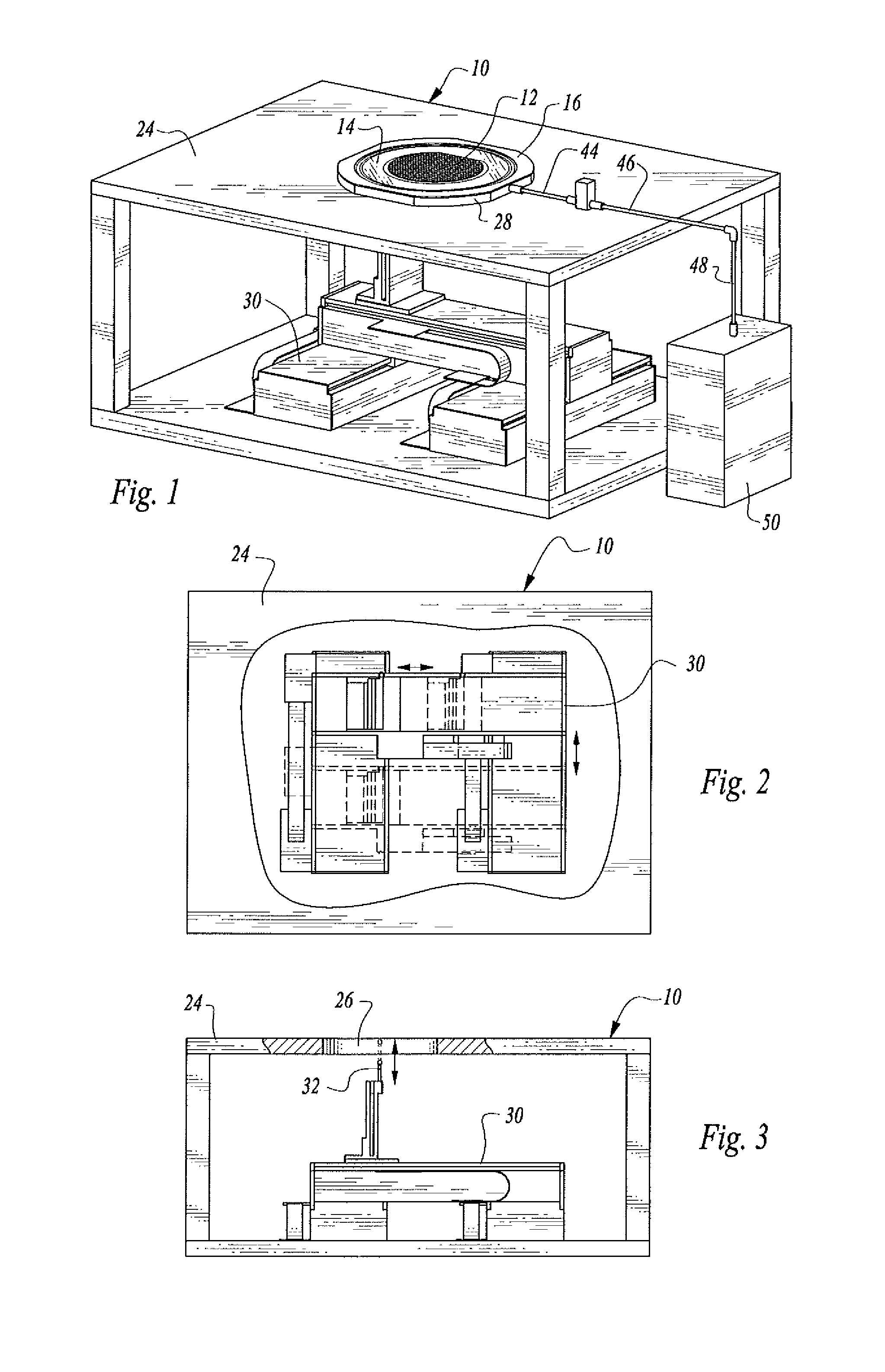
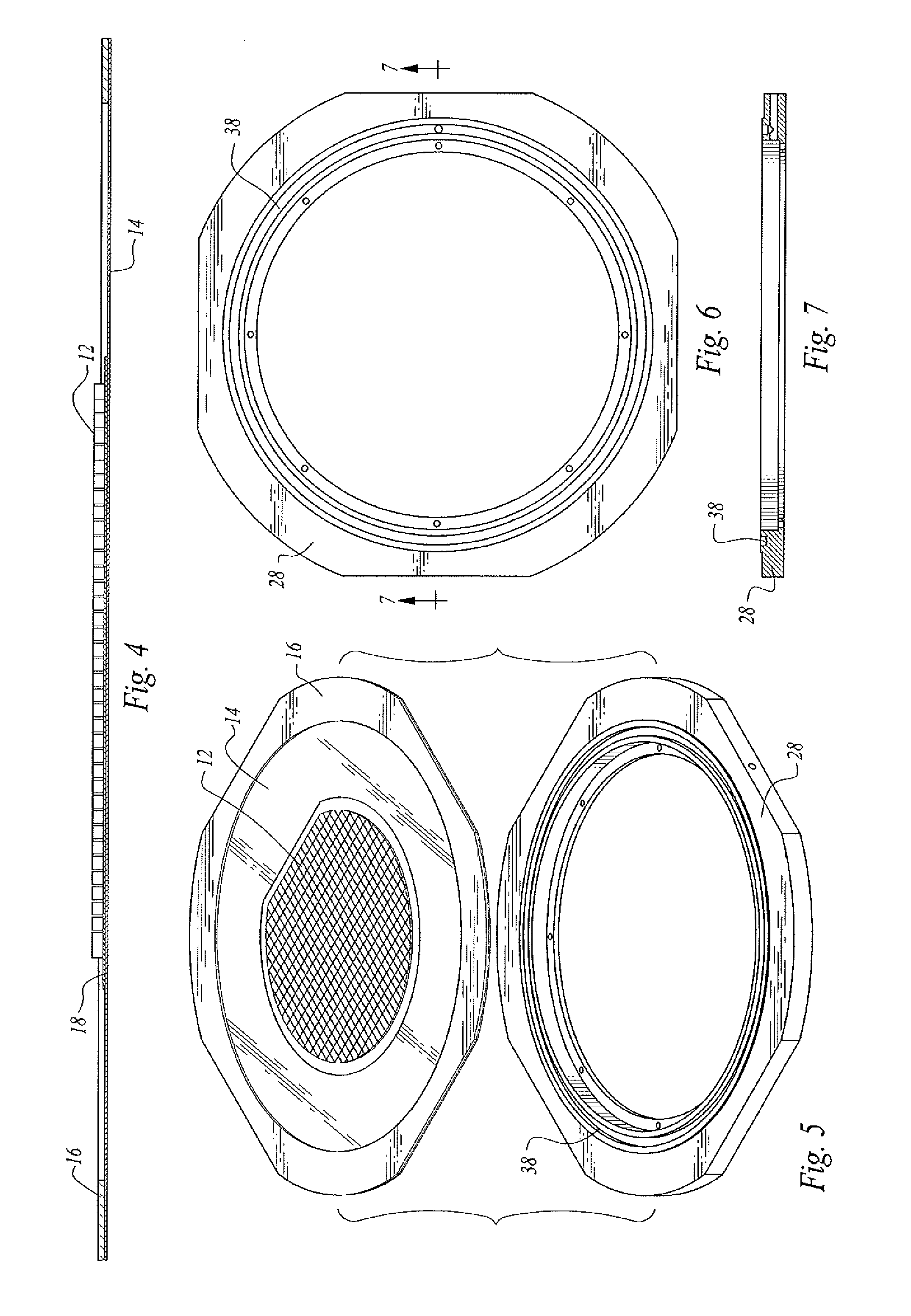
[0036]Referring now to FIGS. 1-12, apparatus utilized to carry out the teachings of the present invention is illustrated and designated by reference numeral 10. The apparatus is for separating semiconductor devices from a semiconductor wafer including back metal on the back side thereof positioned on a plastic film. Such a wafer is designated by reference numeral 12. FIGS. 1, 4, 5 and 8-12 show a plastic film 14 on which the back side of the semiconductor wafer is positioned. As is conventional, a support frame 16 (see FIGS. 4, 5, 8 and 9) supports a peripheral portion of the plastic film surrounding the wafer, as is conventional practice.

[0037]Back metal 18 of the wafer is positioned on the film as is also conventional practice. In the condition shown in the drawings, the wafer is in a condition wherein a rapid, anisotropic etching process has been used to remove all of the semiconductor material in the scribe streets, the etching process having been continued until the back metal ...

second embodiment

[0045]FIGS. 13-18 illustrate apparatus utilized to carry out the steps of the method of this invention wherein the stretch and tension of the plastic film is variable and controlled as a function of a control parameter.

embodiment 10

[0046]Apparatus 60 includes a support table 62 defining an opening (not shown) therein, which may be the same shape as opening 26 of the first apparatus embodiment 10. Below the support table 62 and the opening is a three-axis motion system 30 for moving a stylus (not shown) the same or similar to that incorporated in apparatus 10. The three-axis motion system and stylus operate in the manner of the first apparatus embodiment.


PUM


Abstract

A system for separating semiconductor devices from a wafer having back metal exposed in scribe streets of the wafer positioned on a plastic film by applying a variable radial force to stretch and tension the film while controlling the stretch and tension as a function of a control parameter.

Description

TECHNICAL FIELD[0001]The present invention relates to an apparatus and method for separating semiconductor devices from a semiconductor wafer, and more particularly to separating devices from a wafer having back metal on the backside thereof positioned on a plastic film.BACKGROUND OF THE INVENTION[0002]In the past, numerous different approaches have been used for singulating or dicing a semiconductor wafer, the process of dividing a semiconductor wafer into individual devices. The two most widely used methods at this time are sawing using a diamond saw blade and laser scribing using a focused laser beam to cut through the wafer. Neither method is ideal. Both result in a significant loss of material during the cutting process. As the size of semiconductor devices get smaller, the width of the line of lost material during the scribing process becomes comparable to the width of the device. If the width of the line of material lost during the scribing process could be made significantly...

Claims


Application Information

Patent Timeline
Patent Type & Authority Patents(United States)
IPC IPC(8): H01L21/00H01L21/78
CPCH01L21/78H01L21/67132
Inventor LINDSEY, JR., PAUL C.
Owner SEMICON COMPONENTS IND LLC
Why Eureka
Try Eureka