
Plug connector having an over-molded contact assembly with a conductive plate between two sets of electrical contacts
a technology of electrical contacts and connectors, which is applied in the direction of coupling device connections, dustproof/splashproof/drip-proof/waterproof/flameproof connections, and coupling protective earth/shielding arrangements, etc., can solve the problem of limiting the size of a particular device and the thickness of such portable media devices, so as to reduce size and cost
- Summary
- Abstract
- Description
- Claims
- Application Information
AI Technical Summary
Benefits of technology
Problems solved by technology
Method used
Image

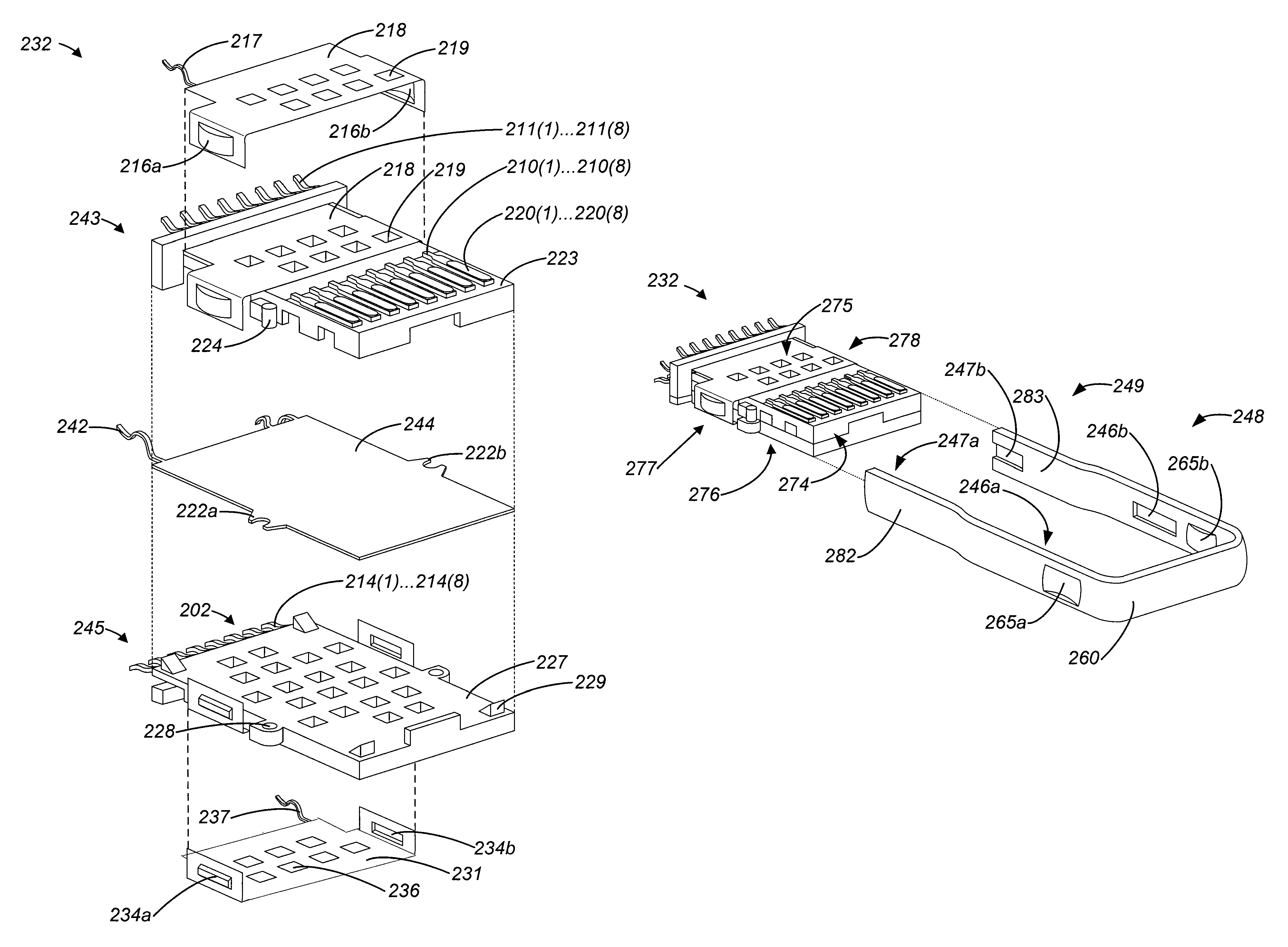
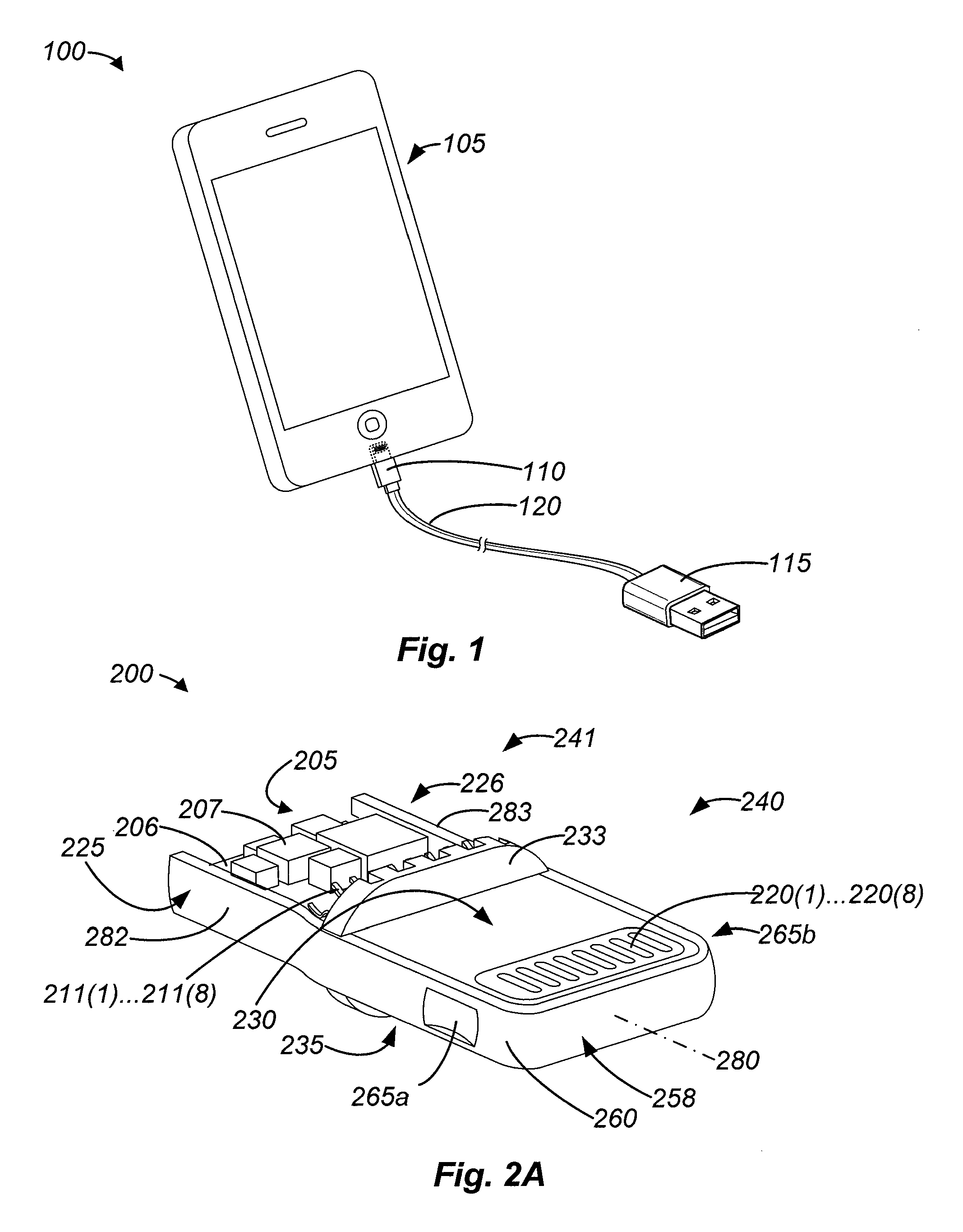
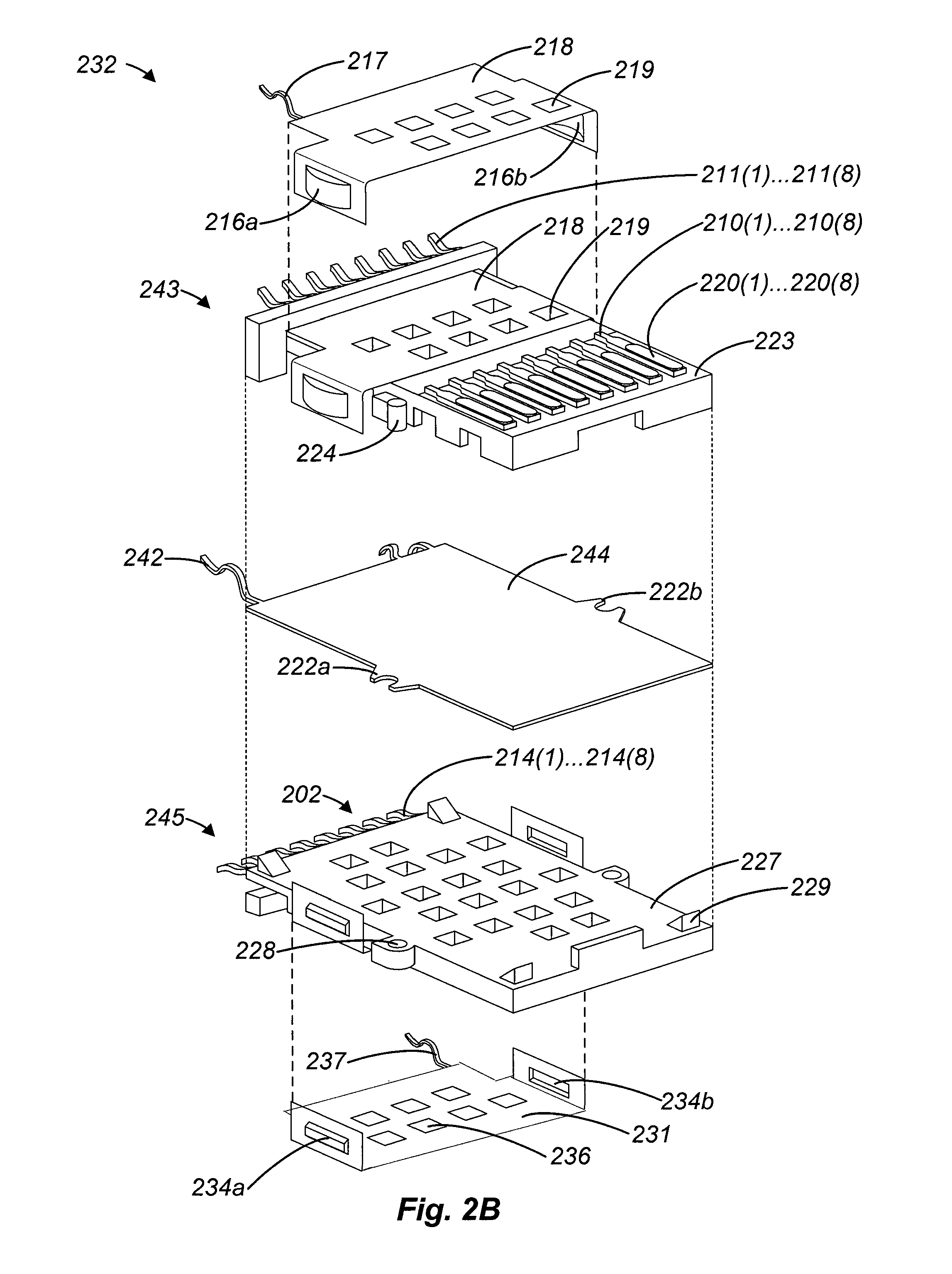
Examples
example electronic
[0055 components 207 are depicted on one side of PCB 206 (see FIG. 2K), however in other embodiments electronic components 207 may be on either or both sides of PCB 206. In some embodiments a conductive epoxy may be used to electrically attach electronic components 207 to PCB 206. In other embodiments a solder alloy may be employed using myriad technologies such as, for example, through-hole mounting, stencil print and reflow, chip-on-board, flip-chip or other appropriate connection method. In one embodiment a stencil printing process is used to dispose solder paste on component bonding pads (not shown). Electronic components 207 may then be disposed on the solder paste and a convective heating process can be used to reflow the solder paste, attaching the electronic components to PCB 206. The solder alloy may be a lead-tin alloy, a tin-silver-copper alloy, or other suitable metal or metallic alloy.
[0056]In some embodiments, during electronic component 207 attachment process, solder ...
PUM
| Property | Measurement | Unit |
|---|---|---|
| thick | aaaaa | aaaaa |
| thick | aaaaa | aaaaa |
| thick | aaaaa | aaaaa |
Abstract
Description
Claims
Application Information