Method of manufacturing semiconductor device

a manufacturing method and semiconductor technology, applied in the direction of semiconductor devices, electrical devices, transistors, etc., can solve the problems of increasing manufacturing costs, increasing the width of resist mask openings, and reducing yield, so as to reduce the alignment accuracy of patterning, increase manufacturing costs, and reduce manufacturing costs

Active Publication Date: 2015-10-20
FUJI ELECTRIC CO LTD
View PDF4 Cites 0 Cited by
  • Summary
  • Abstract
  • Description
  • Claims
  • Application Information

AI Technical Summary

Benefits of technology

[0017]However, in the first conventional method described above, the patterning for forming the resist mask is performed twice, thus increasing manufacturing costs. Furthermore, the patterning to form the resist mask on the rear surface of the semiconductor wafer is performed after the semiconductor wafer has been made thinner. Therefore, the warping of the semiconductor wafer is larger and the alignment accuracy of the patterning is less than it would be if patterning for forming the resist mask were performed on the front surface of the semiconductor wafer. This could lead to increased variation in the widths of the openings on the resist mask and a decrease in yield.
[0018]In the second conventional method described above, the number of patterning steps for forming the resist mask can be reduced to one, but to convert the portion of the p+ area 102 to an n-type, the second ion implantation 123 of phosphorous using the resist mask 122 needs to be performed with a high dose of approximately 4×10¹⁵ / cm2 to 1×10¹⁶ / cm2. The higher the dose of phosphorous is during the second ion implantation 123, the longer that the second ion implantation 123 will take, thus leading to a decrease in throughput of the ion implantation process and an increase in cost.
[0019]Furthermore, the second ion implantation 123 will cause the impurity ions to collide with the resist mask 122 and the kinetic energy the resist mask 122 receives from this collision will increase the temperature of the n− semiconductor wafer 101. The longer the second ion implantation 123 is performed, the more kinetic energy that the resist mask 122 will receive due to the collision with the impurity ions, and thus the rise in temperature of the n− semiconductor wafer 101 will be greater. The heat dissipating characteristics of the semiconductor wafer also become worse the thinner the semiconductor wafer is made. Therefore, if the resist mask is used during ion implantation after the semiconductor wafer has been made thinner as described above, then it will not be possible to avoid a marked increase in temperature caused by the ion implantation as compared to if the same process were being performed with a normal non-thinned semiconductor wafer.

Problems solved by technology

However, in the first conventional method described above, the patterning for forming the resist mask is performed twice, thus increasing manufacturing costs.
This could lead to increased variation in the widths of the openings on the resist mask and a decrease in yield.
The higher the dose of phosphorous is during the second ion implantation 123, the longer that the second ion implantation 123 will take, thus leading to a decrease in throughput of the ion implantation process and an increase in cost.
The heat dissipating characteristics of the semiconductor wafer also become worse the thinner the semiconductor wafer is made.
Therefore, if the resist mask is used during ion implantation after the semiconductor wafer has been made thinner as described above, then it will not be possible to avoid a marked increase in temperature caused by the ion implantation as compared to if the same process were being performed with a normal non-thinned semiconductor wafer.
Thus, the increase in temperature of the semiconductor wafer during ion implantation will cause the organic solvent components constituting the resist mask to become volatile, thereby generating gas (so-called degassing) in the chamber of the ion implantation device and leading to a reduced vacuum level inside the chamber.
This could cause the ion beams to scatter and make it impossible to perform ion implantation at the preconfigured doses, resulting in substantial variation in dose amounts.
The reduced vacuum level in the ion implantation device chamber could be regarded as an abnormality that requires the intervention of a technician or other maintenance, for example, and in such a case, the ion implantation must be aborted.

Method used


Image

  • Method of manufacturing semiconductor device
  • Method of manufacturing semiconductor device
  • Method of manufacturing semiconductor device

Examples


embodiment 1

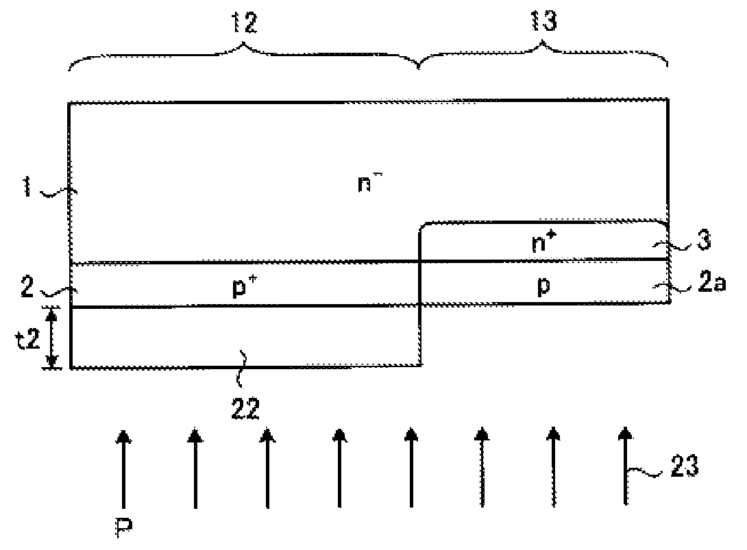
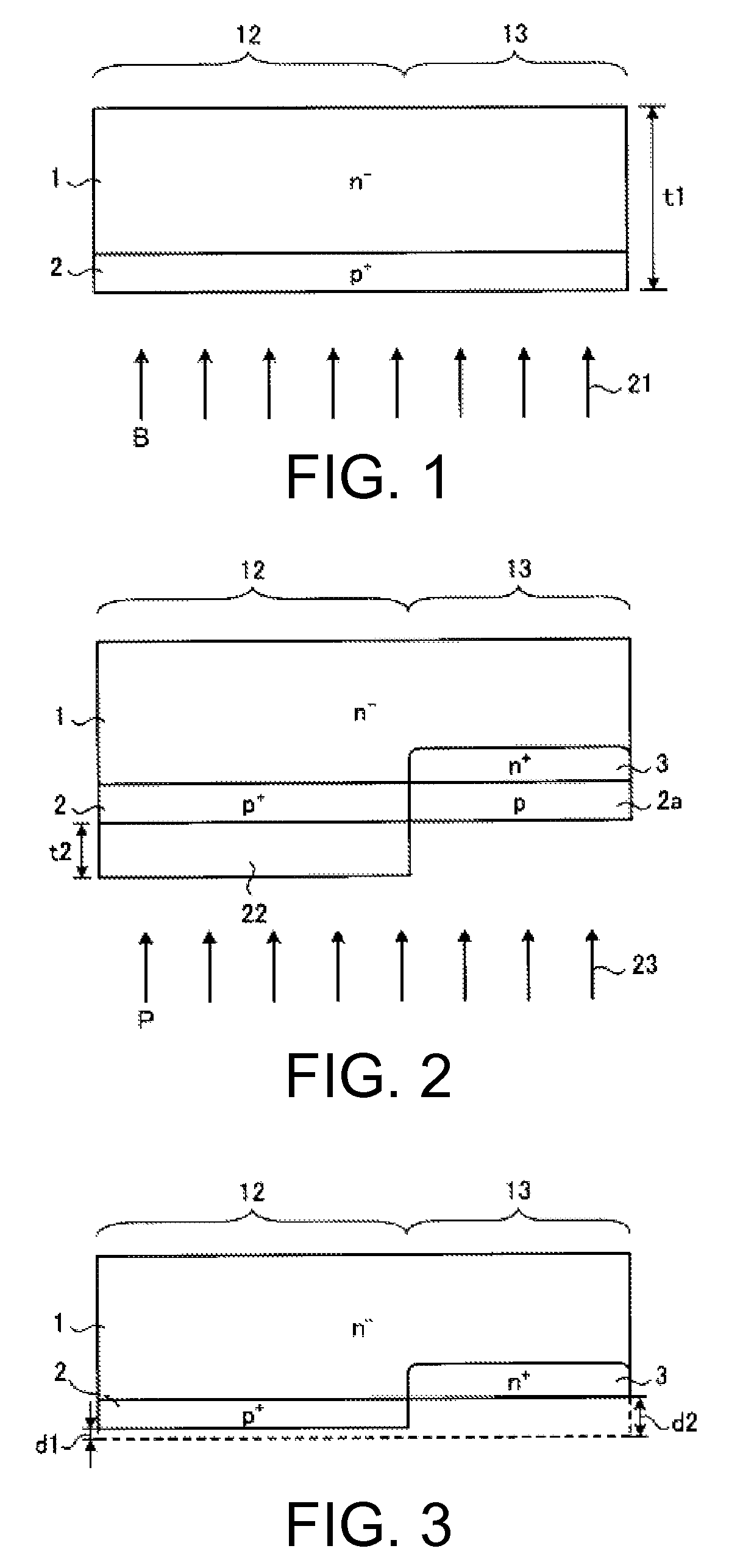
[0046]A method of manufacturing a semiconductor device according to Embodiment 1 will be explained. FIGS. 1 to 3 are cross-sectional views of a semiconductor device of Embodiment 1 during the manufacturing thereof. In FIGS. 1 to 3, the front surface of an n− semiconductor wafer 1 is the top, but the primary surface of the n− semiconductor wafer 1 is flipped as appropriate in the respective steps. Furthermore, in FIGS. 1 to 3, the structure of the front surface side of the n− semiconductor wafer 1 is omitted. An example will be explained in which an RC-IGBT having an IGBT and FWD embedded in the same semiconductor chip is manufactured. In other words, an RC-IGBT is made having a p+ collector region provided on an IGBT area 12 and an n+ cathode region provided on an FWD area 13 on the rear surface of a semiconductor chip formed of the n− semiconductor wafer 1.

[0047]First, as shown in FIG. 1, a front surface element structure (not shown) of an IGBT and FWD is formed by a conventional m...

embodiment 2

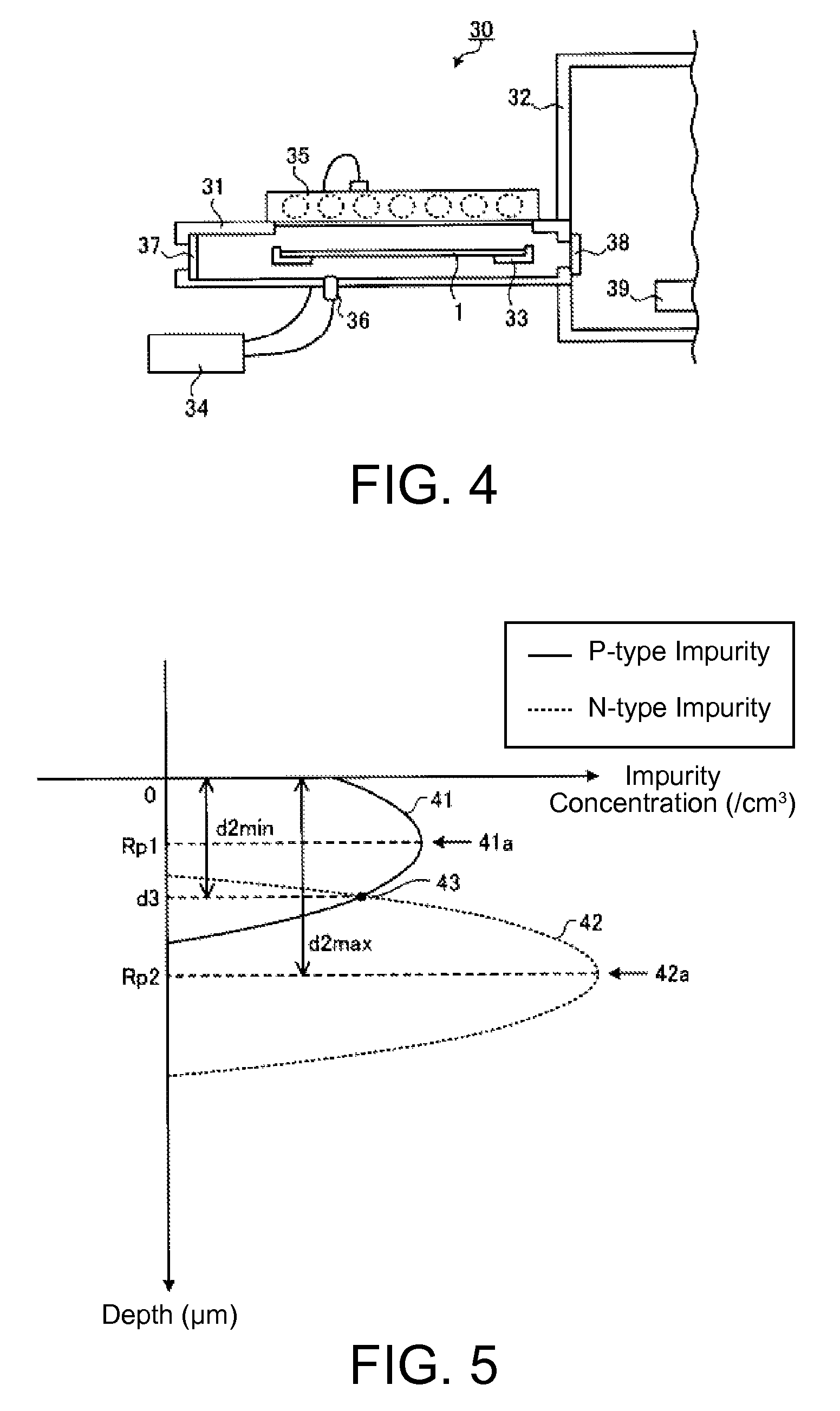
[0073]Next, a method of manufacturing a semiconductor device according to Embodiment 2 will be described. FIG. 7 is a flowchart of an overview of the method of manufacturing a semiconductor device of Embodiment 2. The method of manufacturing a semiconductor device of Embodiment 2 differs from the method of manufacturing a semiconductor device in Embodiment 1 in the calculating scheme of the ashing rate and etching rate of the ashing and etching process.

[0074]As shown in FIG. 7, first an average penetration depth Rp1 and the dose of the p-type impurity during first ion implantation 21 (acceleration energy) are set (step S61). Next, an etching depth d2 of an n− semiconductor wafer 1 rear surface in an FWD area 13 is calculated as described above on the basis of the setting values in step S61 (step S62). Next, an average penetration depth Rp2 and the dose of the n-type impurity during second ion implantation 23 (acceleration energy) are set on the basis of the setting values in step S6...

embodiment 3

[0078]Next, a method of manufacturing a semiconductor device according to Embodiment 3 will be described. The method of manufacturing a semiconductor device of Embodiment 3 differs from the method of manufacturing a semiconductor device of Embodiment 1 in that the ashing and edging process is divided into two steps: performing ashing on a resist mask 22, and performing etching on a silicon part between a rear surface of a n− semiconductor wafer 1 in an FWD area 13 and an n+ area 3.

[0079]Specifically, in a manner similar to Embodiment 1, first the steps from the formation of the front surface element structure to a second ion implantation 23 are performed. Next, the resist mask 22 is removed using a conventional method, such as by performing ashing in an oxygen gas (oxygen plasma) atmosphere, for example. The oxygen atmosphere may have fluorine gas added thereto, in a manner similar to Embodiment 1. Next, the silicon part between the rear surface of the n− semiconductor wafer 1 in th...


PUM


Abstract

When forming a p+ area and n+ area on the same surface of an n− semiconductor wafer, a first ion implantation forms the p+ area on the entire rear surface of the n− semiconductor wafer. Next, a resist mask selectively covering the rear surface of the n− semiconductor wafer is formed. With this resist mask as the mask, an n-type impurity is injected into the rear surface of the n− semiconductor wafer through a second ion implantation to form the n+ area on a portion deeper from the rear surface of the n− semiconductor wafer than the p+ type area. Thereafter, the n− semiconductor wafer is exposed to an oxygen (O2) gas atmosphere with fluorine (F) gas added to remove the resist mask and a silicon part between the rear surface of the n− semiconductor wafer in an FWD area not covered by the resist mask and the n+ area.

Description

BACKGROUND OF THE INVENTION[0001]1. Field of the Invention[0002]The present invention relates to a method of manufacturing a semiconductor device.[0003]2. Description of Related Art[0004]In vertical semiconductor devices such as IGBTs (insulated-gate bipolar transistors) and FWDs (free-wheeling diodes), it is common for the respective semiconductor areas constituting surface element structures to be formed on the surface of a semiconductor wafer, and for p-type or n-type areas to be formed on the rear surface of the semiconductor wafer. In a Reverse Conducting IGBT (RC-IGBT) that has an IGBT and FWD embedded in the same semiconductor chip, for example, both the p-type and n-type areas are formed on the rear surface of the semiconductor wafer.[0005]A well-known method (hereinafter, the first conventional method) of forming the p-type and n-type areas on the rear surface of the semiconductor wafer includes covering the formation area for one of the p-type and n-type areas with a resis...

Claims


Application Information

Patent Timeline
Patent Type & Authority Patents(United States)
IPC IPC(8): H01L29/66
CPCH01L29/66333H01L21/26513H01L21/266H01L21/67115H01L21/67248
Inventor KAMEI, TOSHIHITONOGUCHI, SEIJI
Owner FUJI ELECTRIC CO LTD
Why Eureka
Try Eureka