Memory device and method of controlling leakage current within such a memory device

a memory device and leakage current technology, applied in the field of memory devices, can solve problems such as affecting the performance of read operation, and achieve the effects of improving the speed of operation of coupling circuitry, simple and effective mechanism, and boosting the voltage level of asserted word line signals

Active Publication Date: 2015-10-27
ARM LTD
View PDF22 Cites 36 Cited by
  • Summary
  • Abstract
  • Description
  • Claims
  • Application Information

AI Technical Summary

Benefits of technology

[0015]In accordance with the present invention, reference lines are established, and each column group is associated with one of those reference lines. For each reference line, reference line control circuitry is then used to selectively connect that reference line to the second voltage level, or to disconnect the reference line from the second voltage level. In particular, for each reference line that has an associated column group that is in an active mode of operation (i.e. where a read operation can be performed on an activated memory cell within that column group) the reference line control circuitry connects that reference line to the second voltage level. Conversely, for any reference line that does not have an associated column group in the active mode of operation, that reference line is disconnected from the second voltage level, causing the voltage on that reference line to float, thereby reducing a leakage current path though the coupling circuitry of each memory cell of that associated column group.
[0016]Such an approach significantly reduces the leakage current through the coupling circuitry. However, since the reference line control circuitry will result in an additional component being present in the path between the read bit line and the second voltage level when the associated column group is in the active mode of operation, this could potentially impact the performance of the read operation. To compensate for that potential reduction, the present invention includes word line boosting circuitry configured to generate an asserted word line signal at a boosted voltage level on the read word line, this increasing the performance of the coupling circuitry and ensuring that the presence of the reference line control circuitry does not impact on the read performance. Boosting the read word line voltage can increase read performance significantly, thus allowing the above arrangement to simultaneously achieve both low leakage and high performance.
[0020]The NMOS transistor circuitry can be arranged in a variety of ways. For example, to increase the drive strength, it can be constructed from a plurality of NMOS transistors in parallel between the reference line and the second voltage level. This would ensure that in situations where the associated reference line had an associated column group in the active mode of operation, the NMOS transistor circuitry would operate more strongly to pull the reference line to the second voltage level. However, it would increase the leakage current through the NMOS transistor circuitry in the non-active mode of operation when compared with a weaker NMOS transistor circuitry. In an alternative embodiment, the NMOS transistor circuitry forming the reference line control circuitry may be arranged as a stack of NMOS transistors placed in series between the reference line and the second voltage level. This would decrease the drive strength during the active mode of operation, but would ensure that when the associated reference line did not have an associated column group in the active mode of operation, the stacked arrangement of NMOS transistors forming the reference line control circuitry would improve the leakage current reduction obtainable.
[0023]In such an embodiment, the word line boosting circuitry can be arranged in a variety of ways. However, in one embodiment, the word line driver circuitry includes an inverter circuit whose output forms the read word line pulse signal, and the word line boosting circuitry is configured to boost the voltage across the inverter circuit for at least part of the period that the read word line pulse signal is asserted. This provides a simple and effective mechanism for boosting the voltage level of the asserted word line signal to thereby improve the speed of operation of the coupling circuitry.
[0024]In one embodiment, the memory device may further comprise bit line keeper circuitry coupled to each read bit line and configured during a read operation to weakly pull the voltage on each read bit line towards the first voltage level so as to avoid leakage current within the coupling circuitry of the memory cells of the associated memory cell group from causing the voltage on the associated read bit line to transition to said trip voltage level between said first and said second voltage levels whilst the read word line pulse signal is asserted. The bit line keeper circuitry hence ensures that the correct data value is detected by the read operation, by preventing leakage current within the coupling circuitry from potentially causing an incorrect value to be sensed.

Problems solved by technology

However, since the reference line control circuitry will result in an additional component being present in the path between the read bit line and the second voltage level when the associated column group is in the active mode of operation, this could potentially impact the performance of the read operation.

Method used


Image

  • Memory device and method of controlling leakage current within such a memory device
  • Memory device and method of controlling leakage current within such a memory device
  • Memory device and method of controlling leakage current within such a memory device

Examples


Embodiment Construction

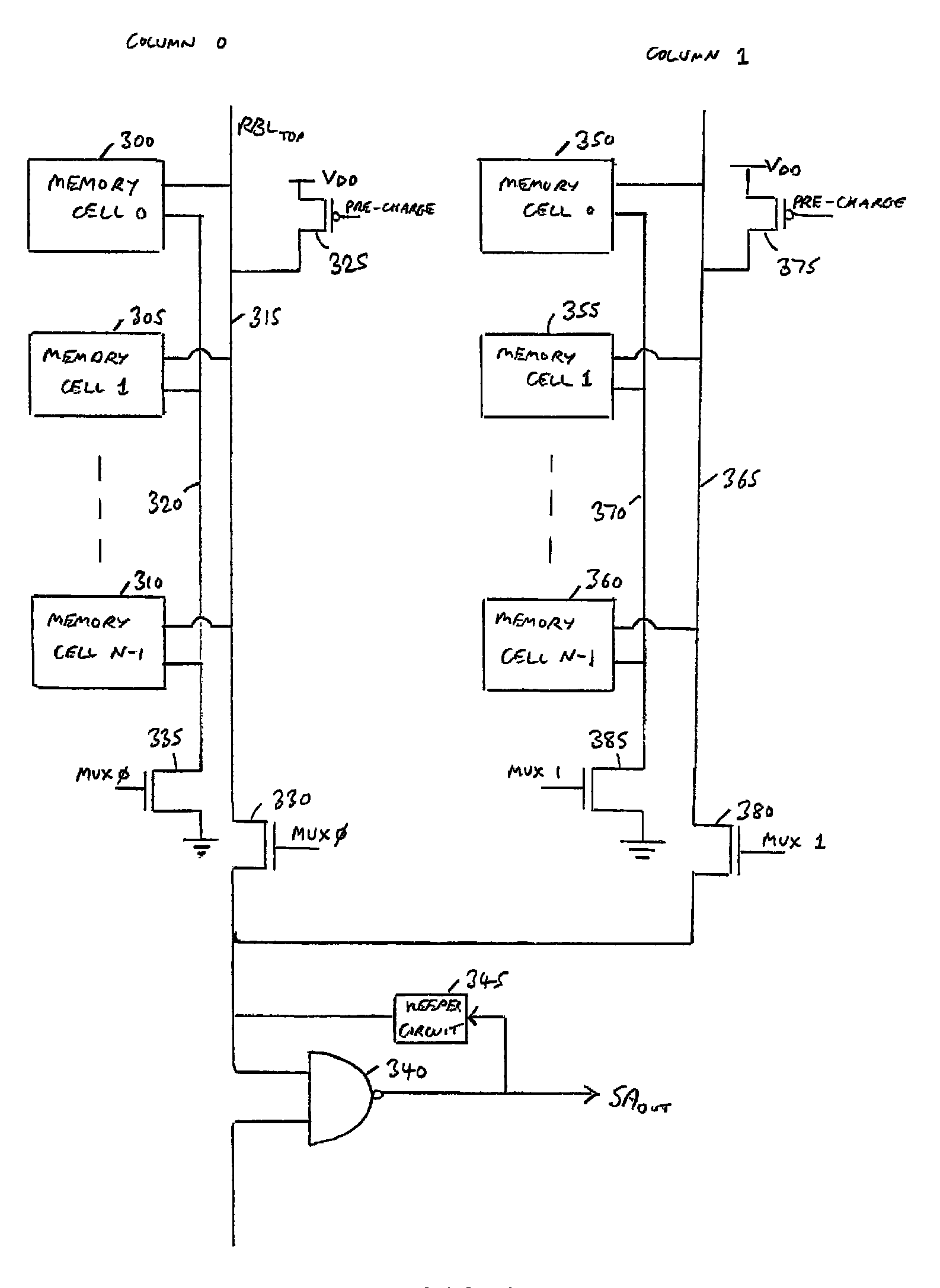
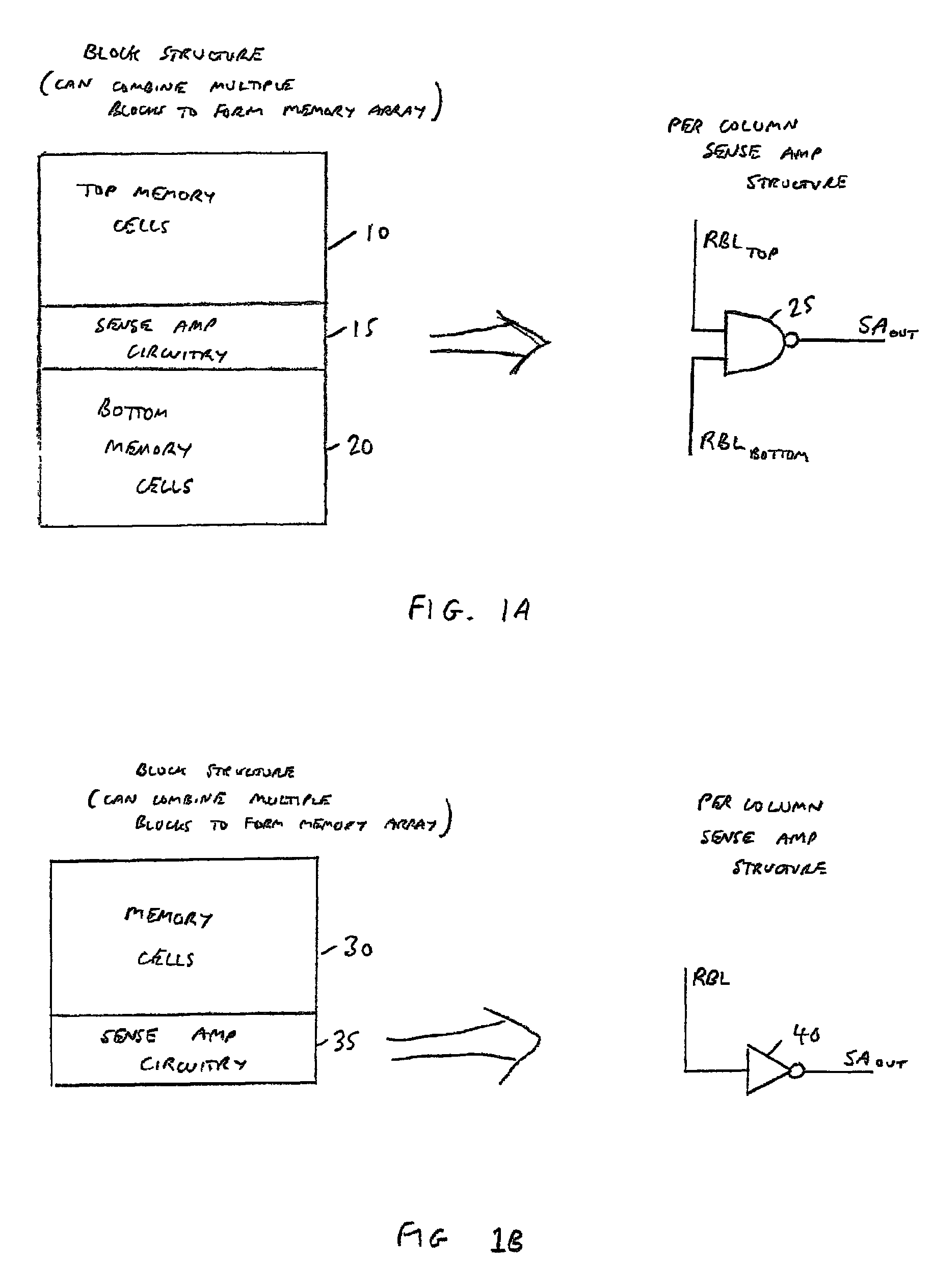
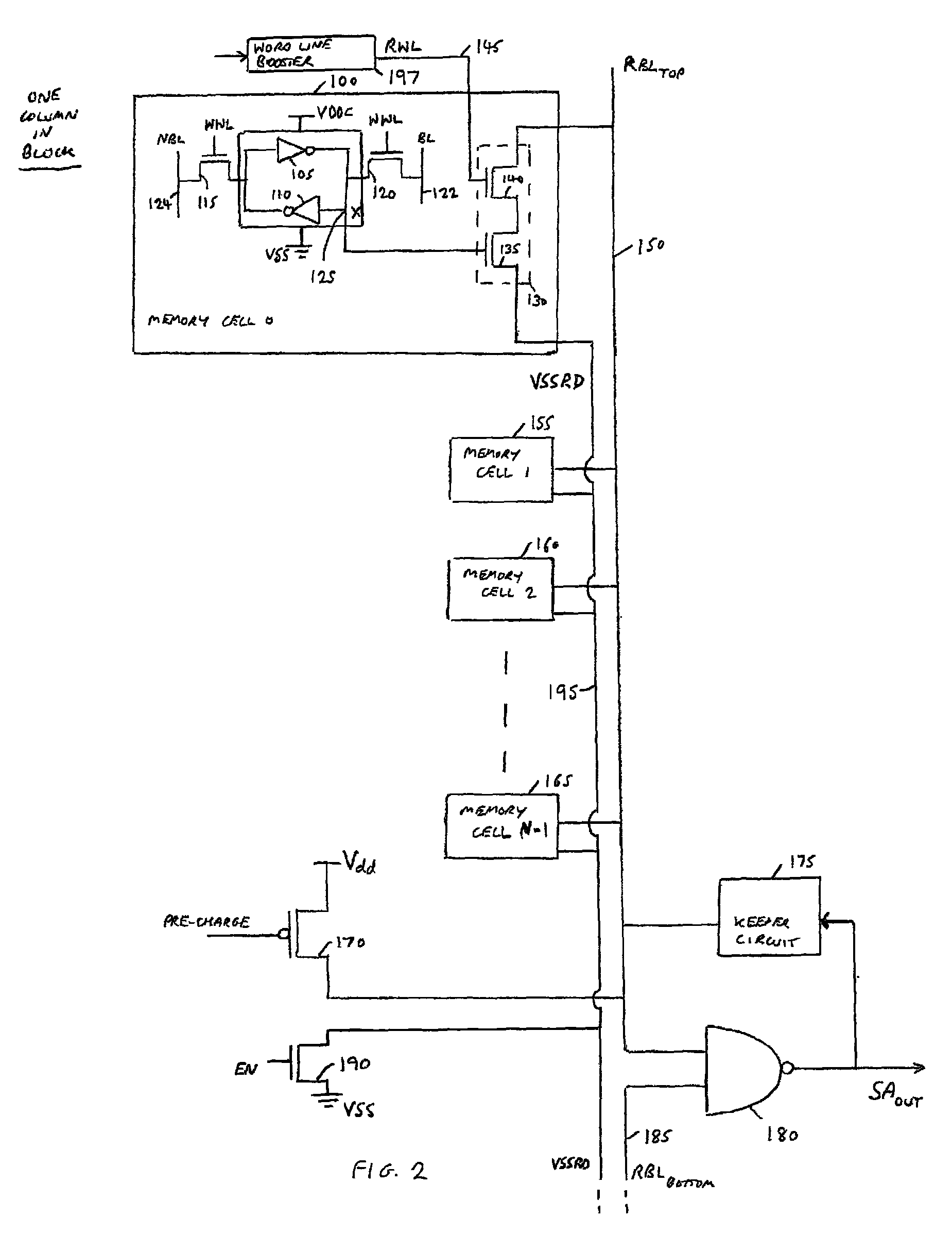
[0042]A memory device in accordance with one embodiment comprises an array of memory cells arranged as a plurality of rows and columns, each row of memory cells being coupled to an associated read word line, and each column of memory cells forming at least one column group, with the memory cells of each column group being coupled to an associated read bit line. The memory array may be constructed using block structures such as shown in FIGS. 1A and 1B. Whilst in one embodiment the memory array may comprise a single block structure, in an alternative embodiment multiple block structures may be used to form the memory array.

[0043]Considering the block structure of FIG. 1A, two memory cell groups are defined, namely a top memory cell group 10 and a bottom memory cell group 20, both of these memory cell groups sharing the same sense amplifier circuitry 15. The top and bottom memory cell groups may provide multiple columns of cells, but each column within a particular memory cell group w...


PUM


Abstract

A memory device includes an array of memory cells arranged as a plurality of rows and columns, each row being coupled to an associated read word line, and each column forming at least one column group, where the memory cells of each column group are coupled to an associated read bit line. Each column has an active mode of operation where a read operation may be performed on an activated memory cell within that column group, and a non-active mode of operation where the read operation is not performable. Precharge circuitry is used, for each column group, to precharge the associated read bit line to a first voltage level prior to the read operation. Each memory cell includes coupling circuitry connected between the associated read bit line and a reference line associated with the column group containing that memory cell.

Description

BACKGROUND OF THE INVENTION[0001]1. Field of the Invention[0002]The present invention relates to a memory device comprising an array of memory cells, and to a method of controlling leakage current within such a memory device.[0003]2. Description of the Prior Art[0004]When developing memory devices, significant development effort is expended in seeking to improve the performance, and / or reduce the power consumption, associated with write and read operations. For example, the articles “A Step-Down Boosted-Wordline Scheme for 1-V Battery-Operated Fast SRAMs”, by H Morimura et al, IEEE Journal of Solid-State Circuits, Volume 33, No. 8, August 1998, Pages 1220 to 1227, “PVT-and-Aging Adaptive Wordline Boosting for 8T SRAM Power Reduction” by A Raychowdhury et al, ISSCC 2010, Session 19, High-Performance Embedded Memory, 19.6, Pages 352 to 354, and “Low Power SRAM with Boost Driver Generating Pulsed Word Line Voltage for Sub-1V Operation” by M Iijima et al, Journal of Computers, Volume 3,...

Claims


Application Information

Patent Timeline
Patent Type & Authority Patents(United States)
IPC IPC(8): G11C16/28G11C11/418G11C7/12G11C8/08G11C11/419
CPCG11C16/28G11C7/12G11C8/08G11C11/418G11C11/419G11C8/12G11C11/412G11C11/413H10B10/12
Inventor ZHENG, BOYEUNG, GUSBOHRA, FAKHRUDDIN ALI
Owner ARM LTD
Why Eureka
Try Eureka