Flexible display device and manufacturing method thereof

a flexible display and manufacturing method technology, applied in semiconductor devices, identification means, instruments, etc., can solve problems such as difficult diversification of design, thin film layer cracking or deterioration, display defects when bent or curved, etc., to improve flexibility and flexibility of flexible substrates, prevent the property deterioration of elements, and form stably elements

Active Publication Date: 2015-11-03
LG DISPLAY CO LTD
View PDF1 Cites 2 Cited by
  • Summary
  • Abstract
  • Description
  • Claims
  • Application Information

AI Technical Summary

Benefits of technology

[0012]The embodiments are to provide a flexible display device which is adapted to enhance flexibility of a flexible substrate and its flexibility by forming the flexible substrate configured with a lower substrate with a prominence pattern and a planarization film, as well a manufacturing method thereof.
[0013]Also, the embodiments are to provide a flexible display device and a manufacturing method thereof which are adapted to prevent property deterioration of elements and stably form the elements by disposing the elements on a prominence pattern of a lower substrate.

Problems solved by technology

Due to this, it is difficult to diversify the design.
However, the flexible display device can cause display defects when bent or curved.
The bending stress forces the thin film layers to be cracked or deteriorated.
Due to this, physical and electrical properties of the electronic elements can deteriorate.

Method used


Image

  • Flexible display device and manufacturing method thereof
  • Flexible display device and manufacturing method thereof
  • Flexible display device and manufacturing method thereof

Examples


second embodiment

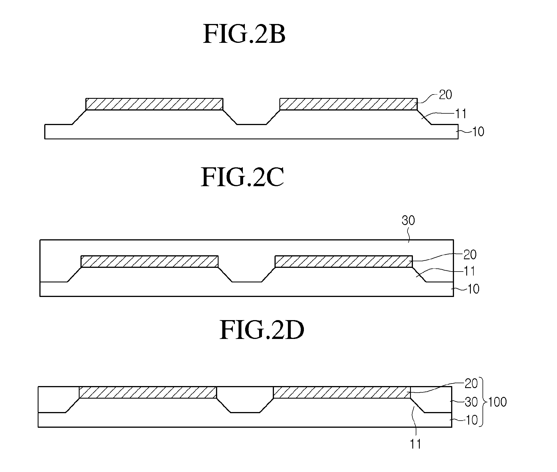
[0030]FIGS. 2A through 2D are cross-sectional views illustrating a method of manufacturing a flexible display device of the present disclosure.

[0031]Referring to FIG. 2A, a barrier layer pattern 20 may be formed on a lower substrate 10. As an example of the lower substrate 10, a plastic thin film, a metal thin film, or others can be used. However, the lower substrate 10 is not limited to theses. In other words, the lower substrate 10 can be formed from any one of flexible materials different from the above-mentioned materials but suitable for the application.

[0032]The barrier layer pattern 20 can be formed from an inorganic material. Actually, the barrier layer pattern 20 can be formed from any one selected from a material group which includes SiO2, SiNx, SiNO, Ge, and mixtures thereof, but it is not limited to these. The barrier layer pattern 20 can be formed from an opaque inorganic material. In this case, the barrier layer pattern 20 can shield light incident to the thin film tr...

third embodiment

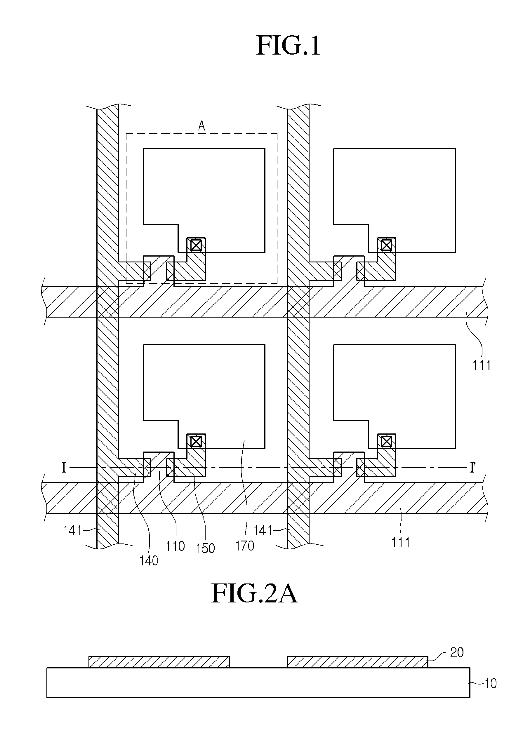
[0047]FIG. 3B is a perspective view showing a second example of the flexible substrate 300 according to the present disclosure. The flexible substrate 300 of the second example includes a barrier layer pattern 20 formed in an island shape and a prominence pattern 11 formed in an island shape. The barrier layer pattern 20 and the prominence pattern 11 which have the island shape can be formed in a region corresponding to a pixel region. In other words, the island pattern can be formed in a region corresponding to a pixel region. As such, the barrier layer pattern 20 and prominence patter 11 can be formed into the same number as the pixel regions. The barrier layer pattern 20 and the prominence pattern 11 each having the island shape can be formed only in a part of the pixel region which is occupied by a thin film transistor. Electronic elements will be formed on the flexible substrate 100.

first embodiment

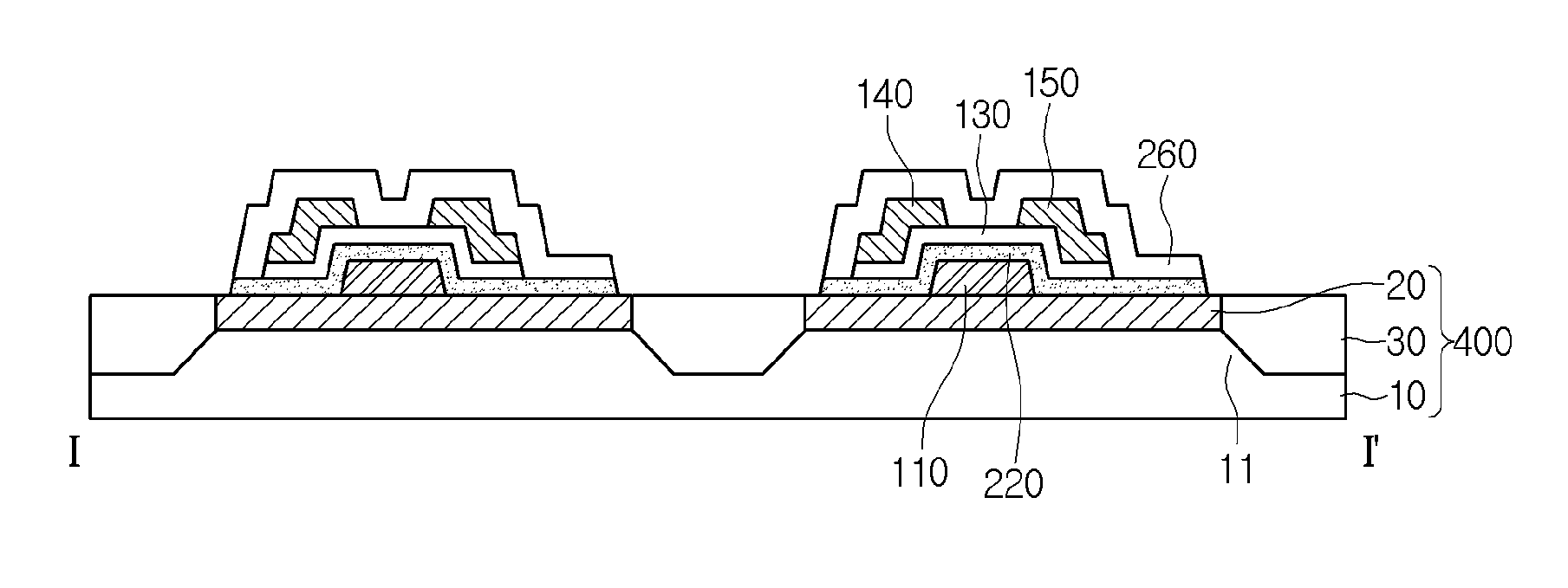
[0048]FIG. 4 is a cross-sectional view along I-I′ from FIG. 1 showing a flexible display device according to the present disclosure.

[0049]As shown in FIG. 4, a gate electrode 110 branched from the gate line is formed on the flexible substrate 400. Also, a gate insulation film 120 can be formed on the entire surface of the flexible substrate 400 provided with the gate electrode 110.

[0050]The gate line and the gate electrode 110 can be formed by stacking at least one metals and transparent conductive materials in at least one layer. The metals include molybdenum Mo, titanium Ti, tantalum Ta, tungsten W, copper Cu, chrome Cr, aluminum Al, and alloys thereof. The transparent conductive materials include ITO (indium-tin-oxide), IZO (indium-zinc-oxide), and ITZO (indium-tin-zinc-oxide). Although the gate electrode 110 is formed in a single metal layer as shown in the drawing, it is not limited to this. In other words, the gate electrode 110 can be formed by stacking at least two metal lay...


PUM


Abstract

A flexible display device includes: a flexible substrate having a lower substrate including a prominence pattern, a barrier layer pattern on the prominence pattern, and a planarization film; a gate line on the flexible substrate; a data line crossing the gate line with having a gate insulation film therebetween to define a pixel region; a thin film transistor formed at an intersection of the gate line and the data line; and a passivation layer on the flexible substrate including the thin film transistor. With this configuration, the flexible substrate and the flexible display device can be enhanced by preventing property deterioration of the elements due to bending stresses.

Description

CROSS-REFERENCE TO RELATED APPLICATION[0001]The present application claims priority under 35 U.S.C. §119(a) to Korean Patent Application No. 10-2013-0116486 filed on Sep. 30, 2013 which is incorporated by reference in its entirety for all purposes as if fully set forth herein.BACKGROUND[0002]1. Field of the Disclosure[0003]The present application relates to a flexible display device and a manufacturing method thereof. More particularly, the present application relates to a flexible display device which allows elements to be stably formed on a flexible substrate and enhances flexibility of the flexible substrate and reliability, and to a method of manufacturing the same.[0004]2. Description of the Related Art[0005]Nowadays, the world has seen rapid advances in the electronic display field for visually representing an information. As a result, a variety of flat panel display devices that are slim, light weight, and with low power consumption have been developed. Also, the flat panel d...

Claims


Application Information

Patent Timeline
Patent Type & Authority Patents(United States)
IPC IPC(8): H01L29/04H01L31/036H01L31/0376H01L21/4757H01L31/20H01L27/12H01L21/47H01L21/471
CPCH01L27/124H01L21/47H01L21/471H01L21/4757H01L27/1225H01L27/1259H01L27/1218H01L27/1262G09F9/30
Inventor PARK, CHANG BUM
Owner LG DISPLAY CO LTD
Why Eureka
Try Eureka