Multiband photodetector utilizing serially connected unipolar and bipolar devices
a multi-band photodetector and serial connection technology, applied in the direction of radiation controlled devices, optical radiation measurement, instruments, etc., can solve the problems of complex tunnel junctions, difficult fabrication of small pitch focal plane arrays (fpa), and more complex electrical switching and electrical connections, so as to reduce the number of optical biasing light sources, reduce the number of tunnel junctions, and simplify the fabrication and operation of multi-band detectors
- Summary
- Abstract
- Description
- Claims
- Application Information
AI Technical Summary
Benefits of technology
Problems solved by technology
Method used
Image
Examples
example 1
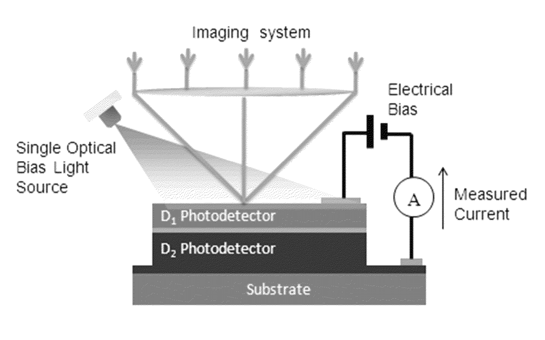
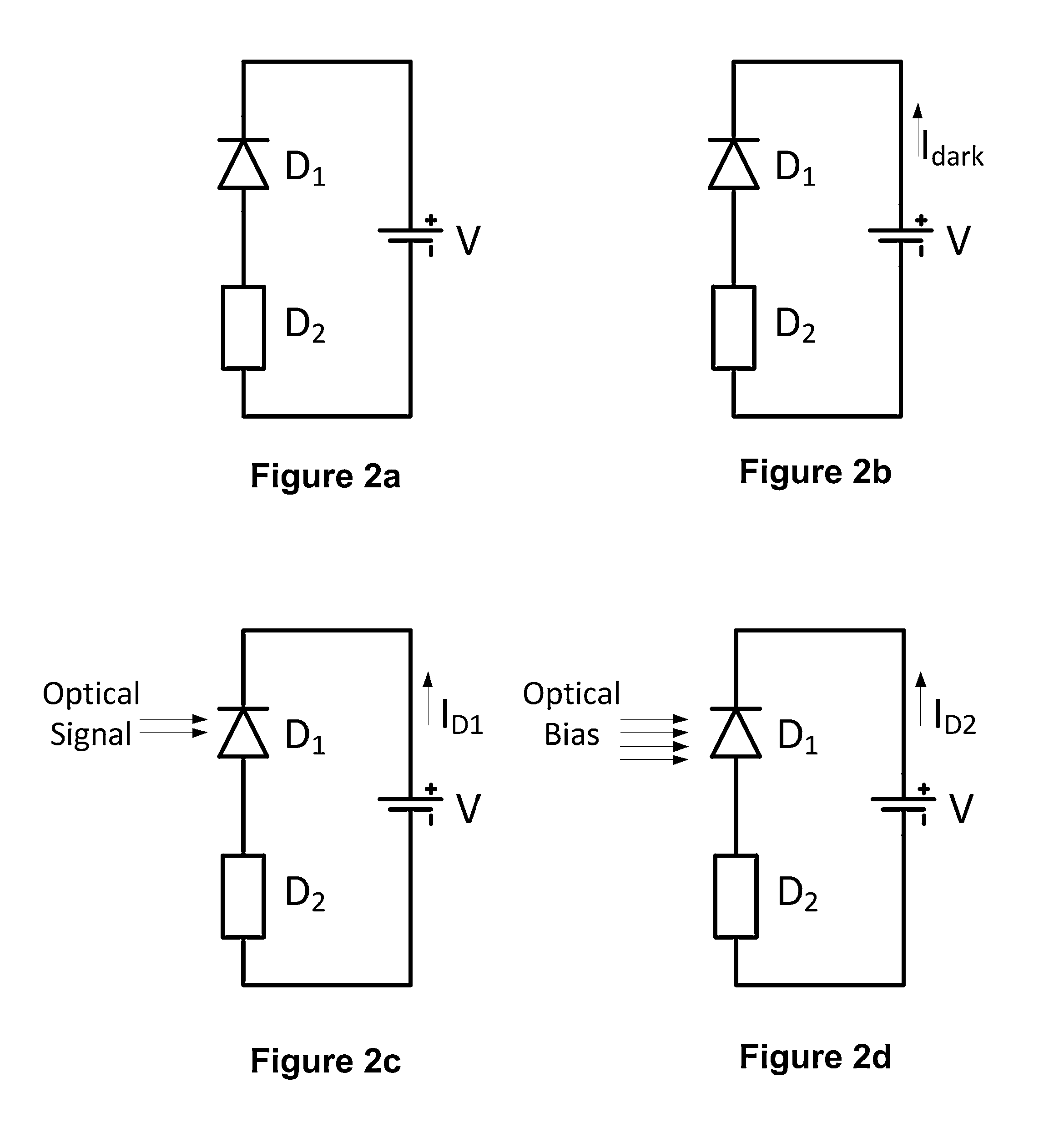
[0116]An NIR PIN photodetector and an LWIR QWIP were connected in series. This proposed device design utilized an 8-9 μm AlGaAs / GaAs LWIR QWIP, and an NIR AlGaAs / GaAs PIN photodiode. Such a combination took advantage of the mature GaAs technology. An exemplar epilayer design for front-side illumination configuration and 77 K operation is shown in Table 2. The shorter wavelength NIR PIN device was designed on top of the LWIR QWIP on a GaAs substrate. The PIN photodetector had a 500 nm AlGaAs window layer, and a 2500 nm thick GaAs intrinsic layer, followed by a 500 nm GaAs n-contact layer. The QWIP was a standard design consisting of 16 times of 4.0 nm GaAs quantum wells sandwiched between 50 nm Al0.27Ga0.73As barriers. The bottom contact layer was 1000 nm thick n-type GaAs. The device was a combination of a bipolar device with a unipolar device and does not need the use of tunnel junctions between them.
[0117]
TABLE 2Front side illuminated device layer structure.LayerdRepeatIDMaterial(...
example 2
[0125]The device was grown with molecular beam epitaxy on (100) GaAs substrate. The QWIP sub-photodetector structure consisted of a 1000 nm thick 1018 cm−3 Si doped n-type GaAs layer for a bottom contact and an absorbing layer consisted of 30 periods of 4.6 nm GaAs quantum wells with 50 nm Al0.27Ga0.73As barriers. The center 4.0 nm regions in the quantum wells were n-doped with Si at 4×1017 cm−3. On top of the QWIP structure, the layers of the p-i-n sub-photodetector were grown in following sequence: 500 nm n-GaAs doped with Si at 1018 cm−3, 2500 nm n-GaAs doped with Si at 2×1016 cm−3 and 400 nm p-Al0.27Ga0.73As window layer doped with C at 1018 cm−3 concentration. The cap layer was a 10 nm p-GaAs doped with C at 1.4×1018 cm−3. The device mesa size 150 μm×150 μm was defined by wet chemical etching. The packaged photodetector was mounted in a cryostat with a ZnSe front window and a quartz side window. The ZnSe front window was used for normal incidence optical response characterizati...
PUM
 Abstract
Description
Claims
Application Information


