Wafer examination device and wafer examination method

a wafer and examination device technology, applied in the direction of individual semiconductor device testing, semiconductor/solid-state device testing/measurement, instruments, etc., can solve the problems of large cost, inability to accurately identify the formation of teg, and inability to accurately measure the electrical properties of the four-point probe method of the related art. , to achieve the effect of high accuracy

Active Publication Date: 2015-12-01
DENSO CORP
View PDF15 Cites 3 Cited by
  • Summary
  • Abstract
  • Description
  • Claims
  • Application Information

AI Technical Summary

Benefits of technology

[0010]The present invention provides a technique that improves a four-point probe method and enables measurement of a silicon carbide wafer by the four-point probe method.
[0012]The probe may include a core of silicon carbide and a coating material which contains the metal and is coated on the core. Further, the metal may include at least one of nickel, titanium, aluminum, chromium, tantalum, molybdenum, tungsten, and cobalt. For example, when the probe of silicon carbide that is coated with nickel is fused to the silicon carbide wafer, nickel diffuses in the silicon carbide wafer, and a nickel silicide alloy (Ni2Si) is formed on an interface between the probe and the silicon carbide wafer. The conductivity between the probe and the silicon carbide wafer is improved by the nickel silicide alloy as a medium, thereby securing an ohmic characteristic.

Problems solved by technology

The four-point probe method of the related art may not be able to accurately measure the electrical property depending on a kind of the silicon wafer (or properties of a layer formed in a wafer shape).
Because the sufficient ohmic characteristic cannot be secured between the probes and the wafer depending on a kind of the silicon wafer, the electrical property of the epilayer may not be accurately measured.
However, formation of the TEG requires large cost.

Method used


Image

  • Wafer examination device and wafer examination method
  • Wafer examination device and wafer examination method
  • Wafer examination device and wafer examination method

Examples


Embodiment Construction

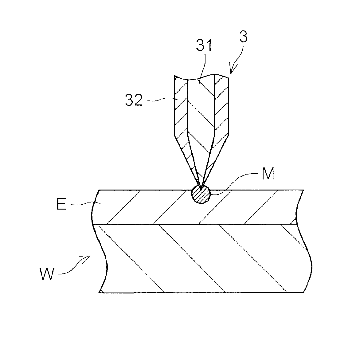
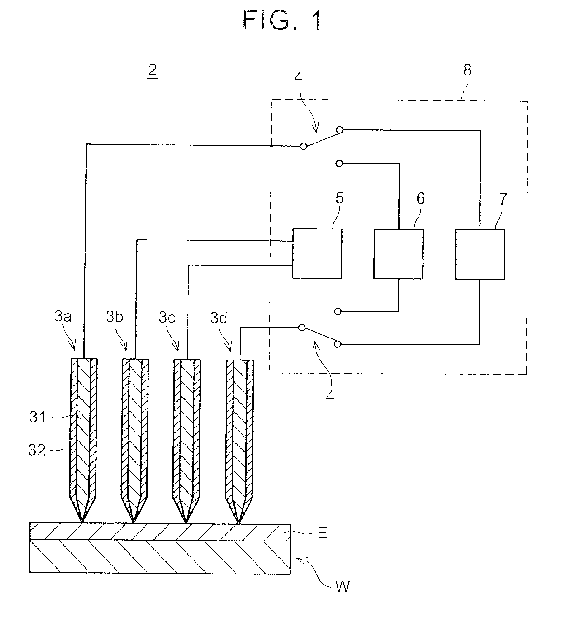
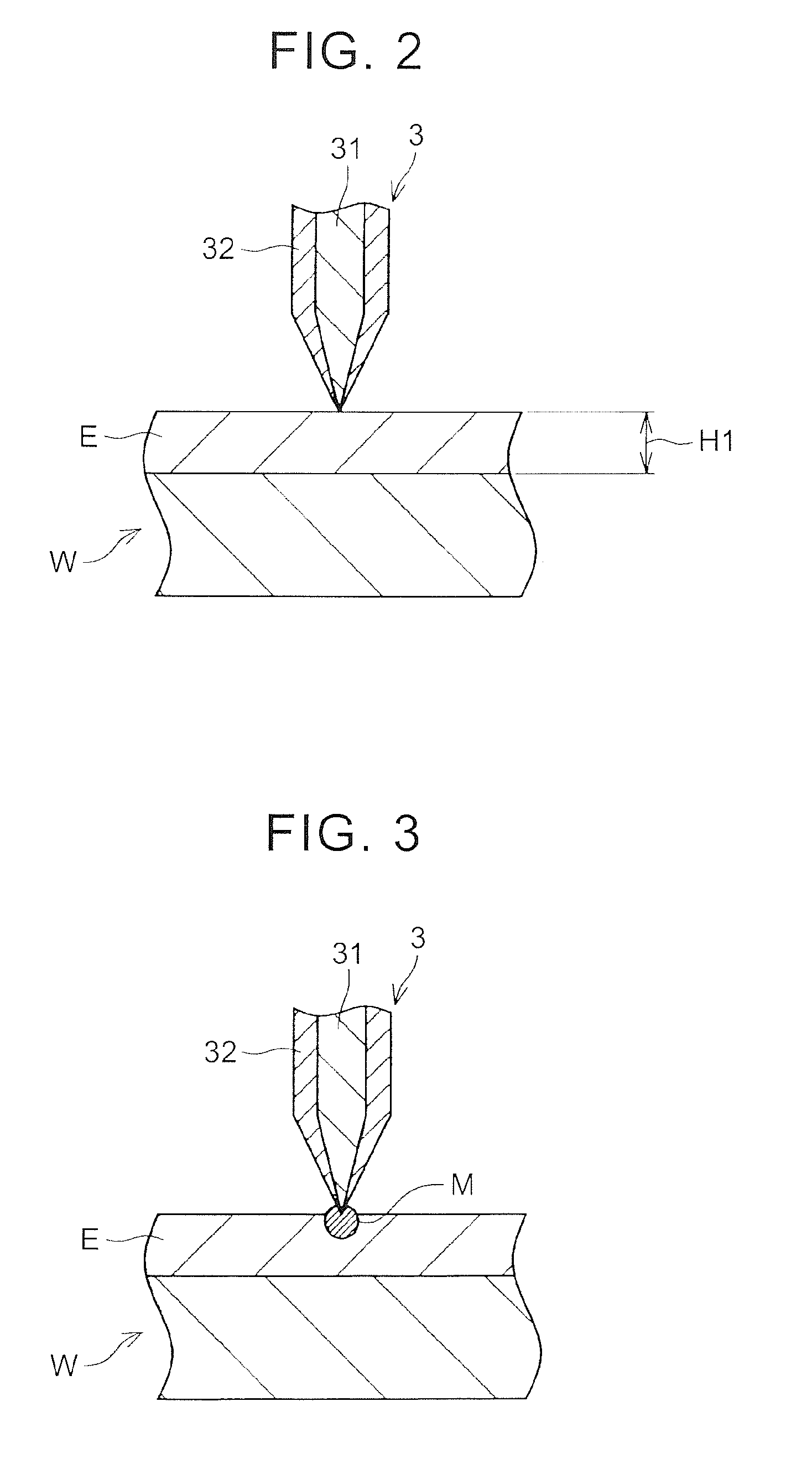
[0022]In an embodiment of the present invention, probes are not simply brought into contact, but special probes are used and fused to a silicon carbide wafer. Conductivity between the probes and the silicon carbide wafer is improved by the fusion, thereby securing an ohmic characteristic. Specifically, probes that can produce a silicide alloy on an interface with the silicon carbide wafer are used to fuse the probes to the silicon carbide wafer. Because the silicide alloy is stable and has high electric conductivity, the ohmic characteristic between the probes and the silicon carbide wafer is improved.

[0023]In the embodiment of the present invention, a silicon carbide wafer on which an epitaxial layer is grown on a surface layer of a substrate is prepared prior to a fusion step. The epitaxial layer is grown by adding a P-type (N-type) dopant to a surface layer of a P-type (N-type) substrate. It should be noted that the substrate may be either one of P-type and N-type and the grown e...


PUM

PropertyMeasurementUnit
thicknessaaaaaaaaaa
thicknessaaaaaaaaaa
thicknessaaaaaaaaaa

Abstract

A wafer examination device includes a probe, a fusion section and a measurement section. The probe is made of a metal which reacts with silicon carbide to produce silicide. The fusion section fuses the probe to a silicon carbide wafer as an examined object. The measurement section measures an electrical property of the silicon carbide wafer through the fused probe.

Description

INCORPORATION BY REFERENCE[0001]The disclosure of Japanese Patent Application No. 2012-269128 filed on Dec. 10, 2012 including the specification, drawings and abstract is incorporated herein by reference in its entirety.BACKGROUND OF THE INVENTION[0002]1. Field of the Invention[0003]The present invention relates to a method for examining an electrical property of a silicon carbide wafer (also referred to as “SiC wafer” or “silicon carbide semiconductor wafer”) and a device for the same.[0004]2. Description of Related Art[0005]In a manufacturing line for forming a semiconductor element on a silicon wafer, the electrical property of the silicon wafer is measured in order to maintain uniform quality. More specifically, an epitaxial layer (epilayer) is grown on the silicon wafer, and the electrical property of the epilayer is measured. The electrical property is typically the resistivity of the epilayer or the resistance value in a predetermined distance in the epilayer.[0006]A four-poi...

Claims


Application Information

Patent Timeline
Patent Type & Authority Patents(United States)
IPC IPC(8): G01R1/06G01R31/20G01R1/067G01R31/00G01R31/26H01L21/66H01L21/44G01N27/20G01R31/02G01R1/04G01R31/28
CPCG01R1/06755G01N27/20G01R1/0491G01R1/067H01L22/00G01R31/2648G01R31/2831G01R31/2886G01R31/00
Inventor FUJIWARA, HIROKAZUSOEJIMA, NARUMASA
Owner DENSO CORP
Why Eureka
Try Eureka