Supercharge Your Innovation With Domain-Expert AI Agents!

Embedded semiconductor device package and method of manufacturing thereof

a semiconductor device and embedded technology, applied in the direction of inspection/indentification of circuits, printed circuit aspects, printed circuit non-printed electric components association, etc., can solve the problems of high cost slow and time-consuming application, and limited reliability of encapsulant/embedding compound typically used

Active Publication Date: 2015-12-08
GENERAL ELECTRIC CO
View PDF19 Cites 20 Cited by
  • Summary
  • Abstract
  • Description
  • Claims
  • Application Information

AI Technical Summary

Benefits of technology

The solution enhances reliability, reduces manufacturing costs, and enables miniaturization by forming robust electrical and thermal connections within the package, improving system-level performance and compatibility with surface mount technology.

Problems solved by technology

For example, the encapsulants and embedding compounds that are generally used have limited reliability when moisture sensitivity level (MSL)-qualification is required, due to their poor fracture toughness and high moisture uptake.
Additionally, the encapsulants / embedding compounds typically used can be expensive to procure and slow and time consuming to apply.
Furthermore, and with particular regard to packaging power devices / modules, the soldering operation typically employed for electrically and thermally connecting the POL sub-module to the ceramic substrate can be costly and time consuming, with the additional temperature excursion required by soldering also adversely affecting module reliability.
Still further, the inclusion of the ceramic substrate in the POL package places limits on an achievable reduction in size and thickness of the POL package (i.e., miniaturization) due to the size / thickness of the ceramic substrate.

Method used


Image

  • Embedded semiconductor device package and method of manufacturing thereof
  • Embedded semiconductor device package and method of manufacturing thereof
  • Embedded semiconductor device package and method of manufacturing thereof

Examples


Embodiment Construction

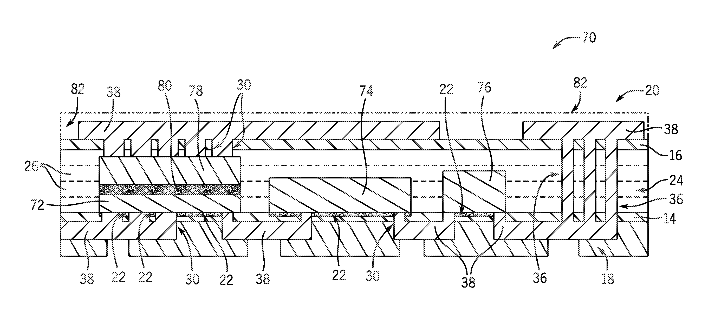
[0025]Embodiments of the present invention provide for an embedded power module package structure having power overlay (POL) interconnects that form all electrical and thermal interconnections to the semiconductor devices in the power module, as well as a method of forming such a package structure.

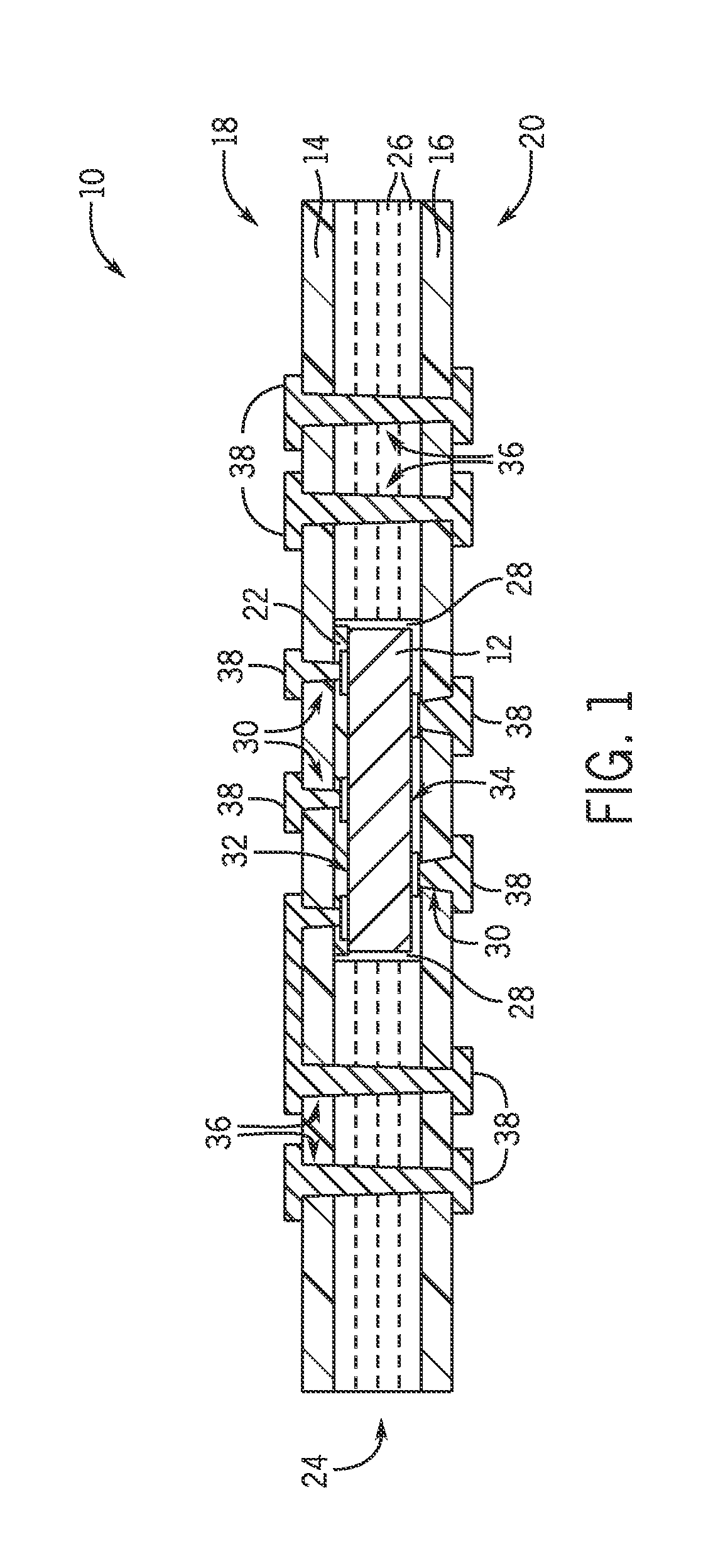
[0026]Referring to FIG. 1, a POL packaging and interconnect structure 10 is shown according to an embodiment of the invention. The package structure 10 includes a semiconductor device 12 that can be in the form of either what can generally be described as a “power device” or a “non-power device”, and thus can be in the form of a die, diode, MOSFET, application specific integrated circuit (ASIC), or processor, for example. While a single semiconductor device 12 is shown in FIG. 1, it is recognized that additional semiconductor devices or electronic components could be included in the POL structure 10, as will be described below regarding another embodiment of the invention. The semiconducto...


PUM


Abstract

A package structure includes a dielectric layer, at least one semiconductor device attached to the dielectric layer, one or more dielectric sheets applied to the dielectric layer and about the semiconductor device(s) to embed the semiconductor device(s) therein, and a plurality of vias formed to the semiconductor device(s) that are formed in at least one of the dielectric layer and the one or more dielectric sheets. The package structure also includes metal interconnects formed in the vias and on one or more outward facing surfaces of the package structure to form electrical interconnections to the semiconductor device(s). The dielectric layer is composed of a material that does not flow during a lamination process and each of the one or more dielectric sheets is composed of a curable material configured to melt and flow when cured during the lamination process so as to fill-in any air gaps around the semiconductor device(s).

Description

BACKGROUND OF THE INVENTION[0001]Embodiments of the invention relate generally to structures and methods for packaging semiconductor devices and, more particularly, to an embedded package structure having power overlay (POL) interconnects that form all electrical and thermal interconnections in the package.[0002]Surface-mount technology is a method for constructing electronic circuits in which surface mount components or packages are mounted directly onto the surface of printed circuit boards (PCBs) or other similar external circuits. In the industry, surface-mount technology has replaced the through-hole technology construction method of fitting components with wire leads into holes in the circuit board.[0003]One common technique for surface-mounting a semiconductor device (or a multi-chip module) is to provide a package structure in which the device / module is encapsulated within an embedding compound. The package manufacturing process begins with placement of one or more semicondu...

Claims


Application Information

Patent Timeline
Patent Type & Authority Patents(United States)
IPC IPC(8): H01L23/48H01L23/00H01L23/538H05K1/18H01L29/40H01L23/52H01L23/34H05K3/46H05K1/02H05K3/30
CPCH01L24/26H01L23/34H01L23/5389H01L24/24H01L24/25H01L24/82H05K1/185H01L2224/73267H01L2224/8201H01L2224/82031H01L2224/82039H01L2224/82047H01L2224/82101H01L2224/83005H01L2224/83132H01L2224/83192H01L2224/83855H01L2224/92144H01L2924/1203H01L2924/13091H01L2924/1433H01L2924/15747H01L2924/15787H05K1/0266H05K3/305H05K3/4602H05K3/4605H05K3/4688H05K2201/0187H05K2203/0278H05K2203/063H05K2203/166H01L2224/04105H01L2224/12105H01L2224/2402H01L2224/24137H01L2224/24195H01L2224/24225H01L2224/2518H01L2224/2732H01L2224/27416H01L2224/291H01L2224/2919H01L2224/32225H01L2224/32245H01L2924/014H01L2924/00H01L2924/181H01L2924/12042H01L23/3677H01L23/5384H01L23/42H01L23/433H01L2224/06181H01L2224/83191H01L2224/96H01L23/367H01L23/3736H01L23/5226H01L23/528H01L23/53228H01L23/53295H01L23/5386H01L24/32
Inventor CHAUHAN, SHAKTI SINGHMCCONNELEE, PAUL ALANGOWDA, ARUN VIRUPAKSHA
Owner GENERAL ELECTRIC CO
Features
  • R&D
  • Intellectual Property
  • Life Sciences
  • Materials
  • Tech Scout
  • Unparalleled Data Quality
  • Higher Quality Content
  • 60% Fewer Hallucinations
Learn More