
Inspection arrangement

a technology of inspection arrangement and inspection surface, applied in the direction of measurement devices, material analysis through optical means, instruments, etc., can solve the problems of interference with the measurement itself, assembly also requires a large aperture and accordingly much space, and the determination of the position of the sample surface is limited

Active Publication Date: 2015-12-22
HSEB DRESDEN
View PDF15 Cites 1 Cited by
  • Summary
  • Abstract
  • Description
  • Claims
  • Application Information

AI Technical Summary

Benefits of technology

[0033]It is advantageous if the portion of the inspected surface illuminated by the incident beam is large enough to detect a reflection averaged over possible structures on the inspected surface. Thereby, effects of roughness will be reduced. The proportion of the illuminated surface and the size of the structure can be easily adjusted by collimation and the distance between the radiation source and the inspected surface.
[0034]The detector may be a Charge-Coupled-Device (CCD), a CMOS or another array detector with high spacial resolution or the detector comprises position sensitive photodiodes or quadrant diodes. Preferably, the used detectors are electrooptical array cameras detecting a high resolution image of the reflected image profile selected according to the respective use requirements. The center of gravity of the detected beam image can be determined with known image processing algorithms and thereby the local position of the beam center can be read out with very high accuracy. Alternatively, simpler recording systems, such as, for example, quadrant diodes or position sensitive photodiodes can be used. Quadrant diodes are an assembly of four photodiodes. Position sensitive photodiodes are large area photodiodes where the center location of gravity of the signal is determined by a generated voltage difference of the signals taken at the edges of the active area.
[0039]In a further modification of the present invention the detector surface is positioned in such a way that the detected radiation forms an angle with the surface normal of the detector surface. Thereby, the resolution and the sensitivity of the assembly can be further increased. The smaller the angle of the reflected beam incident on the detector the more the height position signal or the signal of the inclination of the sample is increased. Since the imaging of the beam on an inclined detector area causes an increased ellipticity of the beam profile it is advantageous if the beam profile is specifically adapted at the radiation source by suitable optical elements. If the inspected surface is parallel directed to the direction of the detector surface, the height resolution relative to the detector surface position perpendicular to the reflected beam can be increased by a factor 3 with an angle of incidence of, for example, 20° relative to the inspected surface. The increase of the sensitivity is already a factor 4 at 15°.
[0041]In an embodiment of the assembly a very stiff connection of the radiation source and the detector as well as the inspection system is advantageous. This can be achieved by the selection of high profile diameters.

Problems solved by technology

Such elements may interfere with the measurement itself.
Such optical assembly also requires a large aperture and accordingly much space directly above the measuring position.
Thereby, the determination of the position of the sample surface is limited.

Method used


Image

  • Inspection arrangement
  • Inspection arrangement
  • Inspection arrangement

Examples


Embodiment Construction

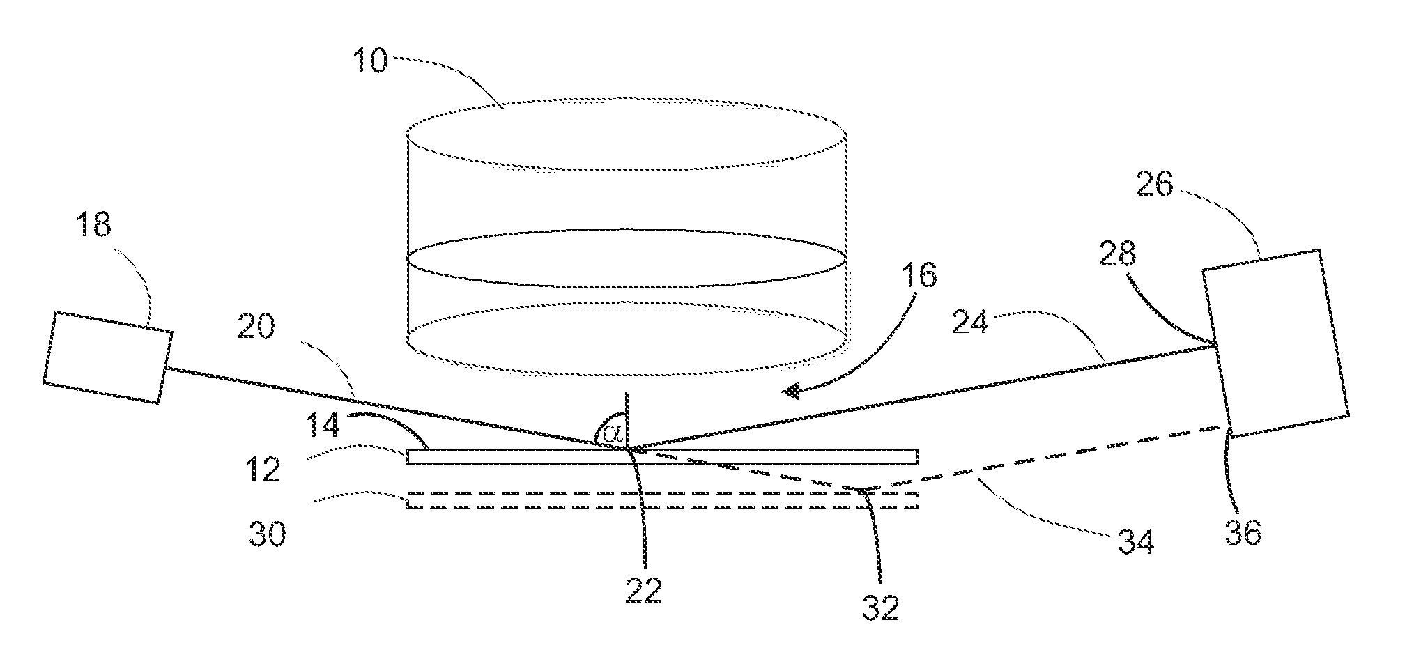
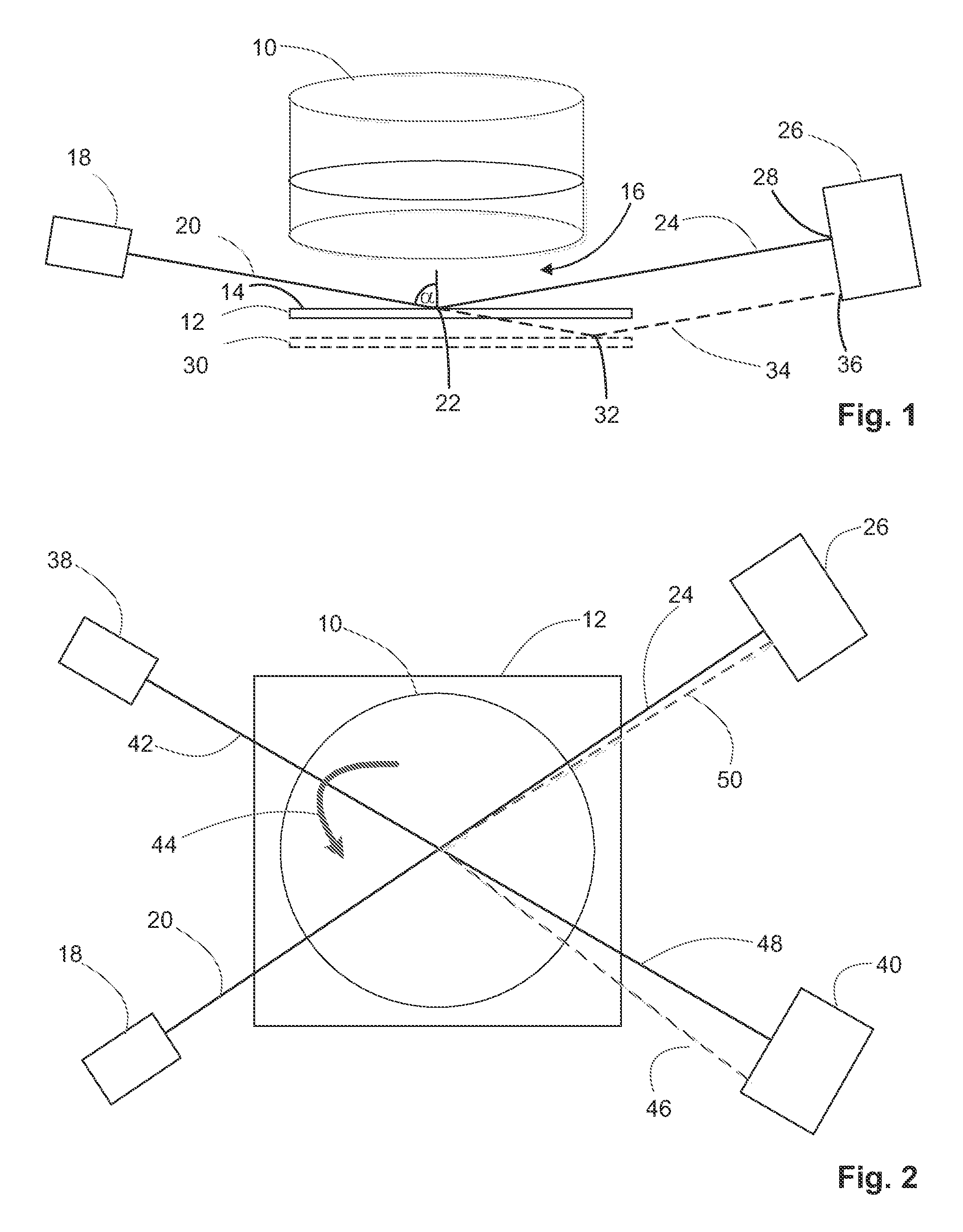
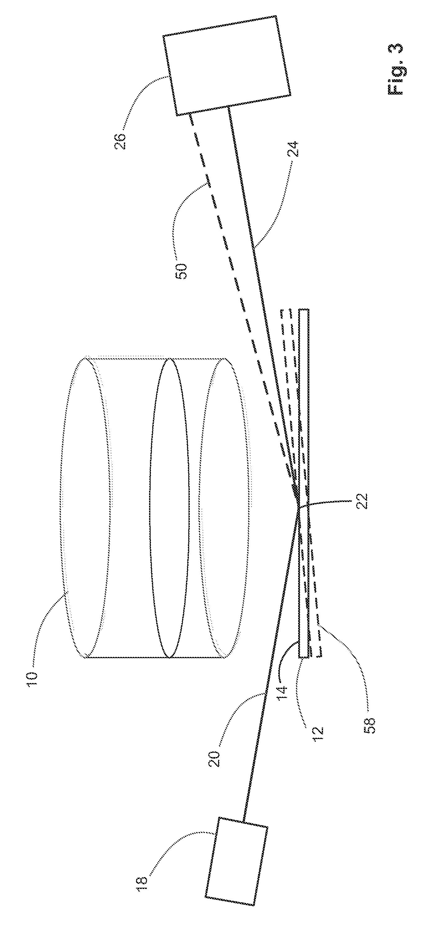
[0052]FIG. 1 shows an inspection assembly for wafers 12 generally denoted with numeral 10. The inspection assembly 10 uses one of the methods ellipsometry, scatterometry, reflectometry, optical inspection, inspection with any other electromagnetic radiation and ultrasound sensorics. The inspection assembly can, however, also apply a photolithographic method.

[0053]The wafer 12 lays on a holder which is not shown here. The holder is designed in such a way that the wafer can be moved in height and also inclined and is equipped with a suitable movement control. Such distance corresponds to the height of the wafer in the present assembly with horizontally positioned wafer. Also, an inclination of the surface 14 can be defined, for example relative to the horizontal plane. The above methods of the inspection assembly are sensitive regarding height and inclination of the wafer.

[0054]Therefore, a measuring assembly for determining the height and inclination of the surface is provided in the...


PUM

PropertyMeasurementUnit
angleaaaaaaaaaa
angleaaaaaaaaaa
anglesaaaaaaaaaa

Abstract

The invention relates to an arrangement for analyzing an at least partially reflective surface of a wafer or other objects, containing a holder for holding the object; an inspection arrangement arranged at a distance in the region in front of the surface to be analyzed; and a measurement arrangement for determining the distance and / or inclination of the surface for the inspection arrangement; characterized be a radiation source, the radiation of which is directed towards the surface to be analyzed at an angle; and a spatially resolving detector for receiving the radiation from the radiation source that is reflected from the surface to be analyzed, wherein the radiation source and the detector are arranged outside the region necessary for the inspection between the inspection arrangement and the surface to be analyzed.

Description

TECHNICAL FIELD[0001]The invention relates to an assembly for inspecting an at least partly reflecting surface of a wafer or other object.[0002]Furthermore, the invention relates to an inspection method for inspecting an at least partially reflecting surface of a wafer or another object with an inspection assembly positioned spaced apart in the range before the inspected surface, the method used for determining the distance and / or inclination of the surface with respect to the inspection assembly.[0003]In different branches of the industry flat products are inspected with optical methods regarding their properties. In semiconductor- and solar cell industry these are amongst others wafers. Wafers are discs of semiconductor-, glass-, sheet- or ceramic materials. The exact determination of the surface position of the sample during various inspection steps is important for the correct performance of the inspection itself and for the correct interpretation of the measuring results. The p...

Claims


Application Information

Patent Timeline
Patent Type & Authority Patents(United States)
IPC IPC(8): G01N21/00G01B11/14G01N21/95G01B11/02G01B11/26G01N21/21
CPCG01B11/14G01B11/026G01N21/9501G01B11/26G01N2201/062G01N21/211
Inventor SROCKA, BERNDLANGHANS, RALF
Owner HSEB DRESDEN
Learn More