Transverse ultra-thin insulated gate bipolar transistor having high current density

a bipolar transistor, ultra-thin technology, applied in the direction of semiconductor devices, semiconductor/solid-state device details, electrical apparatus, etc., can solve the problems of difficult to improve the current density, achieve high current density, improve the current density of the transverse ultra-thin igbt, and increase the current density

Active Publication Date: 2016-01-19
SOUTHEAST UNIV
View PDF5 Cites 165 Cited by
  • Summary
  • Abstract
  • Description
  • Claims
  • Application Information

AI Technical Summary

Benefits of technology

[0008]The transverse ultra-thin IGBT having high current density of the present invention uses a new structure, that is, the N epitaxial layer (3) is provided therein with the P base region array (17) including the P annular base region (6b), and the P base region array (17) is located between the N well region (4) and the P base region (6a). Compared with a conventional transverse ultra-thin IGBT (FIG. 3) having only one P base region, the present invention achieves that after a gate voltage increases constantly, a depletion layer first occurs below the gate oxide layers of the P base region (6a) and the P annular base region (6b), and after the gate voltage reaches a threshold voltage, an inversion layer occurs below the gate oxide layers of the P base region (6a) and the P annular base region (6b), which is equivalent to addition of a conducting channel of a parasitic NMOS transistor in the transverse ultra-thin IGBT, that is, increase of a current of the parasitic NMOS transistor. As shown in FIG. 1, the N epitaxial layer (3) in the x direction and the y direction further can provide a current flow path, and thus the current of the parasitic NMOS transistor can be used as a base region current of a PNP transistor in the transverse ultra-thin IGBT, so that an electro hole collecting capability is added to the first P contact region (7a) and the second P contact region (7b) of the P base region (6a) and the P annular base region (6b). Finally, current density of the transverse ultra-thin IGBT is improved.
[0009](2) Because the P base region (6a) and the P base region array (17) including the P annular base region (6b) cause increase of a quantity of conducting channels, compared with the conventional transverse ultra-thin IGBT having high current density of the present invention has higher current density under the condition of a same withstand voltage, or has a higher withstand voltage under the condition of same current density.
[0010](3) The transverse ultra-thin IGBT having high current density of the present invention is totally based on an existing transverse ultra-thin IGBT manufacturing process, no additional process step is added, and manufacturing is simple.

Problems solved by technology

However, for an ultra-thin L-IGBT, it is very difficult to improve the current density as a conductivity modulation effect is not obvious enough.

Method used


Image

  • Transverse ultra-thin insulated gate bipolar transistor having high current density
  • Transverse ultra-thin insulated gate bipolar transistor having high current density
  • Transverse ultra-thin insulated gate bipolar transistor having high current density

Examples


Embodiment Construction

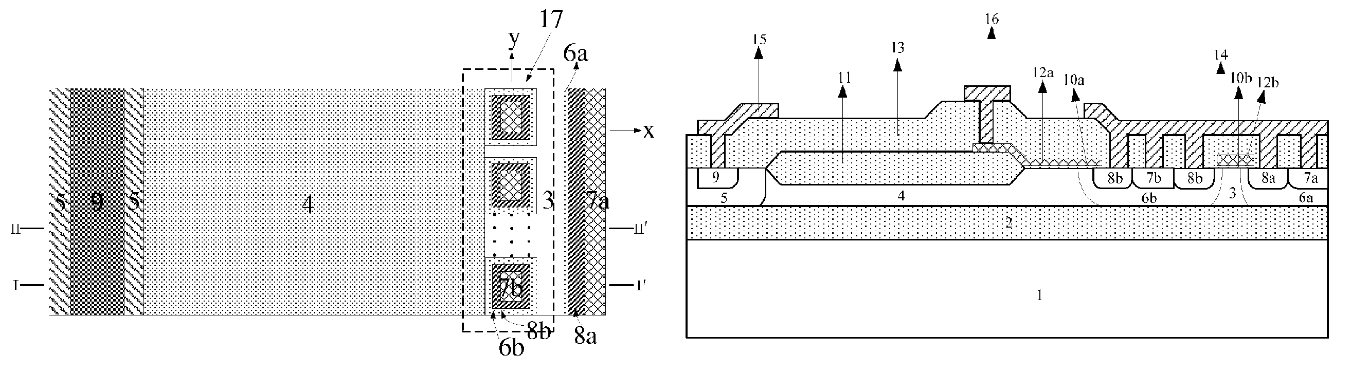
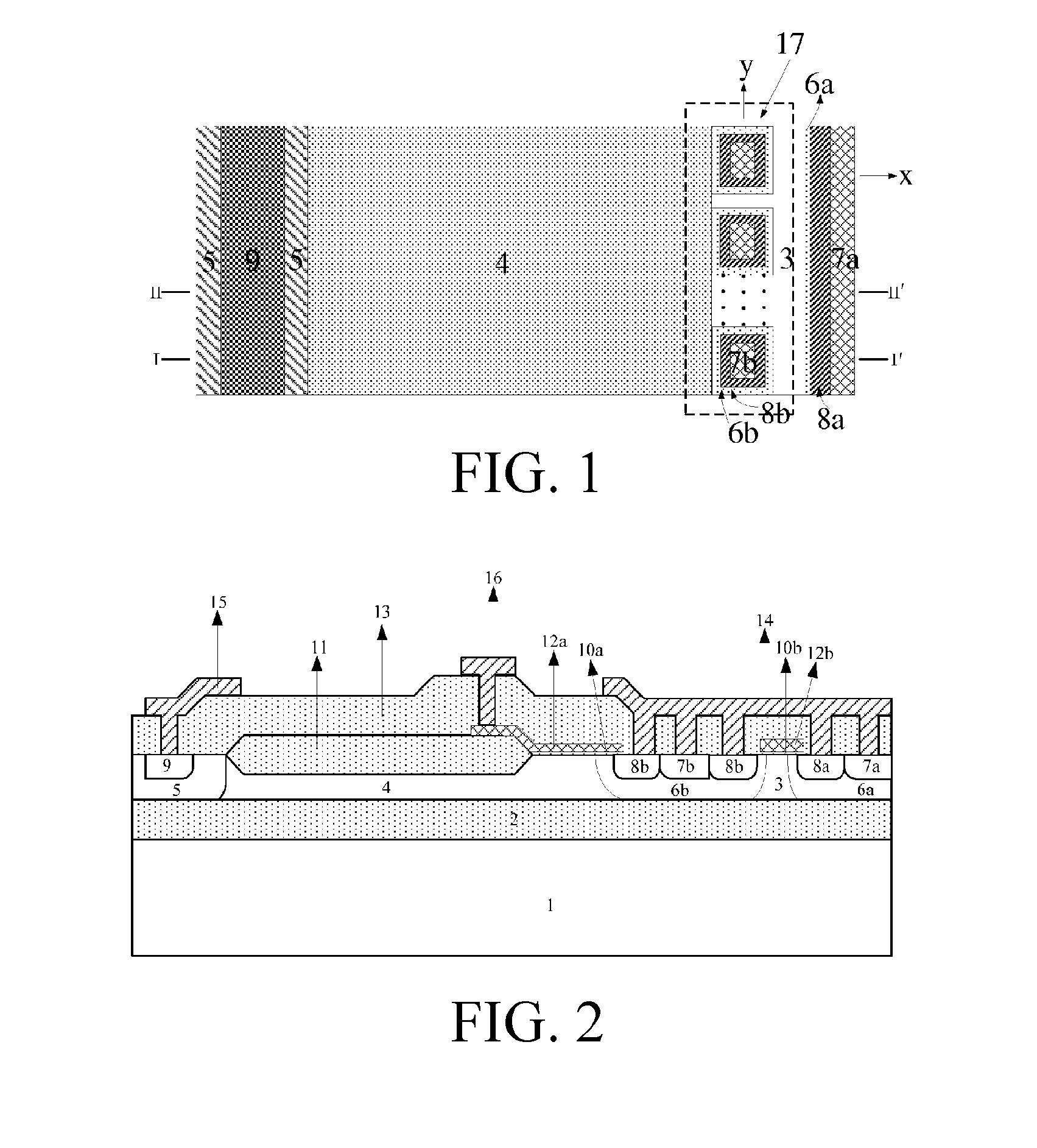
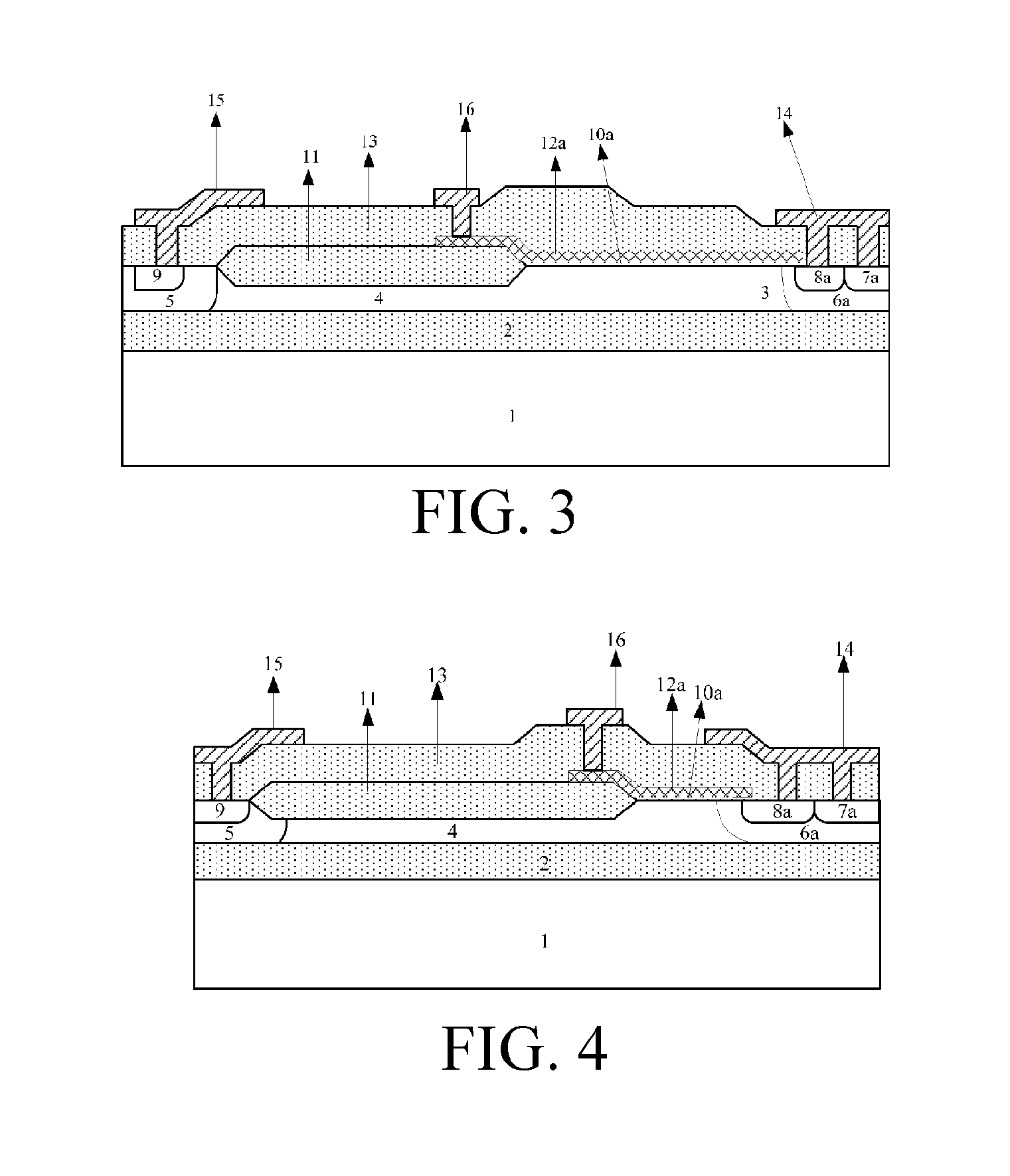
[0019]Referring to FIG. 1, FIG. 2, and FIG. 3, a transverse ultra-thin IGBT having high current density includes: a P substrate 1, where the P substrate 1 is provided with a buried oxide layer 2 thereon, the buried oxide layer 2 is provided with an N epitaxial layer 3 thereon, the thickness of the N epitaxial layer 3 is 0.1 to 1.5 μm, the N epitaxial layer 3 is provided with an N well region 4 and a P base region 6a therein, the N well region 4 is provided with an N buffer region 5 therein, the N well region 4 is provided with a field oxide layer 11 thereon, a boundary of the N buffer region 5 abuts against a boundary of the field oxide layer 11, the N buffer region 5 is provided with a P drain region 9 therein, and the P base region 6a is provided with a first P contact region 7a and an N source region 8a therein, the N epitaxial layer 3 is provided therein with a P base region array 17 including a P annular base region 6b, the P base region array 17 is located between the N well r...


PUM


Abstract

A transverse ultra-thin insulated gate bipolar transistor having current density includes: a P substrate, where the P substrate is provided with a buried oxide layer thereon, the buried oxide layer is provided with an N epitaxial layer thereon, the N epitaxial layer is provided with an N well region and P base region therein, the P base region is provided with a first P contact region and an N source region therein, the N well region is provided with an N buffer region therein, the N well region is provided with a field oxide layer thereon, the N buffer region is provided with a P drain region therein, the N epitaxial layer is provided therein with a P base region array including a P annular base region, the P base region array is located between the N well region and the P base region, the P annular base region is provided with a second P contact region and an N annular source region therein, and the second P contact region is located in the N annular source region. The present invention greatly increases current density of a transverse ultra-thin insulated gate bipolar transistor, thus significantly improving the performance of an intelligent power module.

Description

CROSS-REFERENCE TO RELATED APPLICATIONS[0001]This application is a US National Stage of International Application No. PCT / CN2012 / 087710, filed 27 Dec. 2012, which claims the benefit of a Chinese Application No. CN20101442085.X, filed 7 Nov. 2012, the entire content of which is fully incorporated by reference herein.FIELD OF THE INVENTION[0002]The present invention relates to power semiconductor devices, and in particular, to a transverse ultra-thin insulated gate bipolar transistor (IGBT) having current density that is integrated on an ultra-thin process platform.DESCRIPTION OF RELATED ART[0003]Intelligent power modules in high-voltage power integrated circuits can be applied to various fields, for example, driving and controlling various industrial and civil single-phase and three-phase motors. A power switch element in an intelligent power module is a key part in the entire intelligent power module. As a power switch element, an IGBT not only is characterized by a high working spe...

Claims


Application Information

Patent Timeline
Patent Type & Authority Patents(United States)
IPC IPC(8): H01L29/66H01L29/10H01L29/08H01L29/49H01L23/528H01L29/739H01L29/06
CPCH01L29/7394H01L29/0696H01L29/0847H01L29/0821H01L29/0808H01L29/0611H01L23/528H01L29/1008H01L29/4916H01L2924/0002H01L2924/00
Inventor SUN, WEIFENGZHU, JINGXU, SHENQIAN, QINSONGLIU, SIYANGLU, SHENGLISHI, LONGXING
Owner SOUTHEAST UNIV
Why Eureka
Try Eureka